


 7 / 62

 edfas.org
7
ELECTRONIC DEVICE FAILURE ANALYSIS | VOLUME 18 NO. 1
(a)
(b)
Fig. 3
Emission localization. (a) Si-CCD camera (>2 V). (b)
InGaAs-CCD camera (>1.6 V)
Fig. 4
AFP measurement on NMOS in case 2
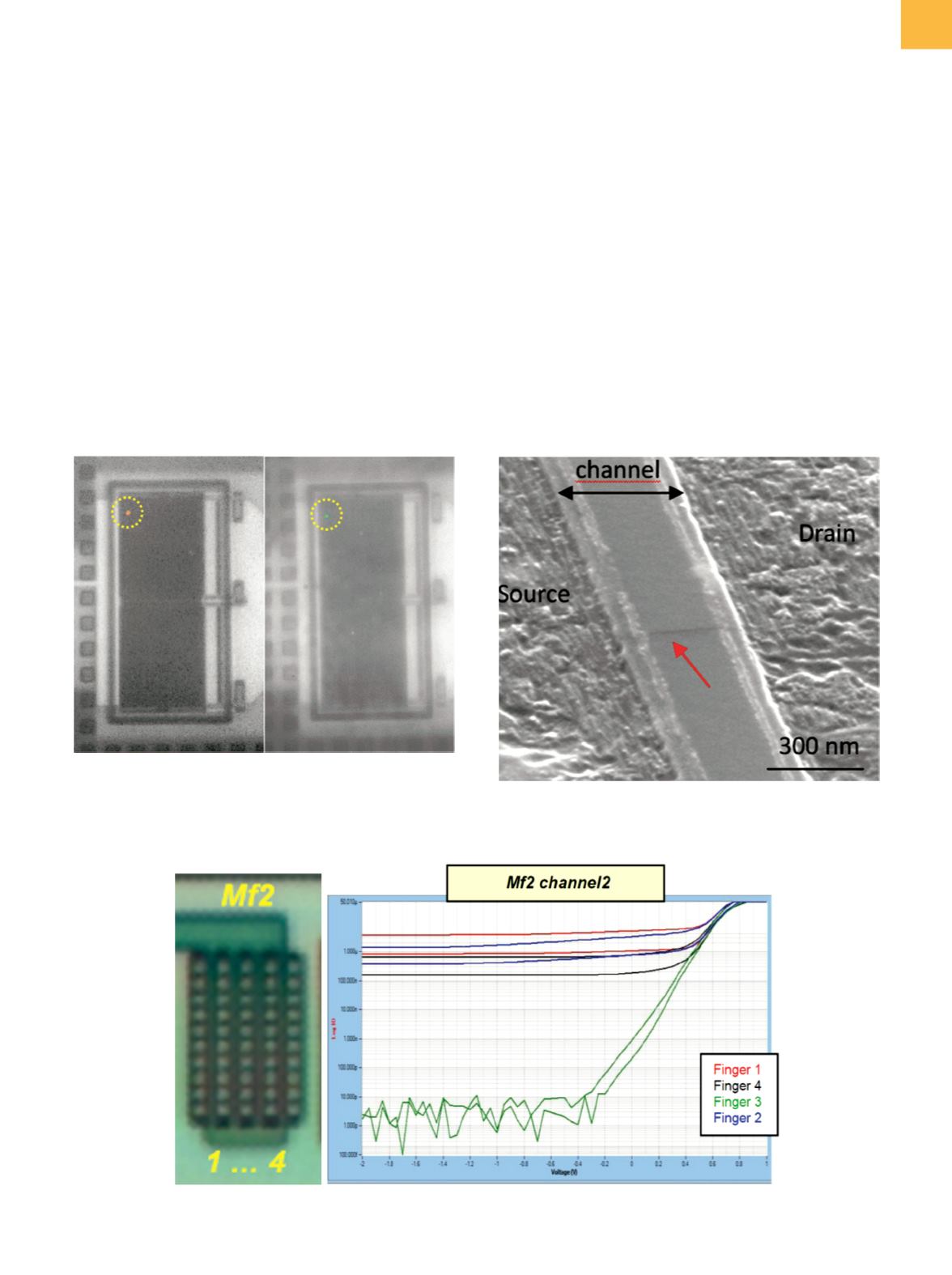
Fig. 5
Tilted SEM image at silicon active area level with PVC
revealing abnormal dark line in channel region
the leakiest patterns, and the defect can extend further
than the TLS/photoemission analysis.
PHYSICAL INVESTIGATIONS
PASSIVE VOLTAGE CONTRAST AT CONTACT LEVEL
Based on the electrical FA findings obtained in case
1, a step-by-step deprocessing was performed to inspect
the metal layers; no anomaly was observed. At contact/
ILD0 level, passive voltage contrast (PVC) was executed
using SEM, confirming that the NMOS polysilicon gate
was properly insulated from the active area. Because the
metal layer and polysilicon gate were not involved in the
NMOS device leakage, it is most likely that a defect at the
silicon level was responsible for the failure.
SILICON ACTIVE AREA SEM INSPECTION
AND PVC
Deprocessing was done by removing the polysilicon
and gate oxide layers to expose active silicon for SEM
inspection. No silicon damage (indicative of ESDdamage)
was observed, and no wafer fab defect (such as micro-
masking or a silicon topography issue) was identified.
Low-acceleration-voltage PVC was performed to provide
different contrast imaging between differently doped
regions.
[7]
A narrow, straight dark linewas observed at the
NMOS channel area. This hairline passed across all the
NMOS channels, and its position and configuration (paral-
lel to one side of the device structure) exactlymatched the
OBIRCH signature (Fig. 5). In the PVC images, the
n
-type
region is darker than the
p
-type area; the observed dark