


 2 / 62

 edfas.org
ELECTRONIC DEVICE FAILURE ANALYSIS | VOLUME 18 NO. 1
2
PURPOSE:
To provide a technical condensation of
information of interest to electronic device failure
analysis technicians, engineers, and managers.
Felix Beaudoin
Editor/Globalfoundries;
felix.beaudoin@ globalfoundries.comScott D. Henry
Publisher
Mary Anne Fleming
Manager, Technical Journals
Annie Beck
Production Supervisor
Liz Marquard
Managing Editor
ASSOCIATE EDITORS
Michael R. Bruce
Consultant
David L. Burgess
Accelerated Analysis
Lihong Cao
Advanced Micro Devices
Jiann Min Chin
Advanced Micro Devices Singapore
Edward I. Cole, Jr.
Sandia National Labs
James J. Demarest
IBM
Christopher L. Henderson
Semitracks Inc.
Jason M. Higgins
TSMC (Wafertech)
Bobby Hooghan
Weatherford Laboratories
Eckhard Langer
Globalfoundries
Philippe H.G. Perdu
CNES France
Rose M. Ring
Globalfoundries
H.S. Silvus, Jr.
Southwest Research Institute
E. Jan Vardaman
TechSearch International, Inc.
Martin Versen
University of Applied Sciences Rosenheim, Germany
Lawrence C. Wagner
LWSN Consulting Inc.
GRAPHIC DESIGN
www.designbyj.comPRESS RELEASE SUBMISSIONS
magazines@asminternational.orgElectronic Device Failure Analysis™
(ISSN 1537-0755) is pub-
lished quarterly by ASM International
®
, 9639 Kinsman Road,
Materials Park, OH 44073; tel: 800.336.5152; website: edfas.
org.Copyright©2016byASM International.Receive
Electronic
Device Failure Analysis
as part of your EDFAS membership
of $88 U.S. per year. Non-member subscription rate is $135
U.S. per year.
Authorizationtophotocopy itemsfor internalorpersonaluse,
orthe internalorpersonaluseofspecificclients, isgrantedby
ASM Internationalfor librariesandotherusersregisteredwith
theCopyrightClearanceCenter(CCC)TransactionalReporting
Service, provided that the base fee of $19 per article is paid
directlytoCCC,222RosewoodDrive,Danvers,MA01923,USA.
Electronic Device Failure Analysis
is indexed or abstracted by
Compendex, EBSCO, Gale, and ProQuest.
T
o understand how great the risk of failure analysis (FA) and debug
techniques is to electronic hardware security, one should look more
closely at what is donewhile applying FA to a digital circuit. We analyze
the digital signal and study the failure mode with, for example, scan path
testing, but that is just the beginning of the investigation. We also start to
extract analog information and evaluate signal levels, current profiles, and
so on. If all of this does not lead us to isolate the failure, then physical inter-
action becomes our focus in order to trace the signal and identify the failing
node. Many of these techniques show not only failing locations but logical
states and perfectly operating signal tracks as well. The tools and practices
that help us with FA on the flip side also enable hackers to gain access to
secret information on the flop side of the IC. The so-called side-channel
attacks (SCAs) read personal codes or passwords to open paths into illegal
IC operation. In addition, circuit edit (CE) opportunities with the focused
ion beam, previously used to gain access to initially secure signals, can be
employed to create ones and zeros in memories such as SRAM by producing
the proper opens and shorts and thereby write and duplicate access codes
into authentication products.
When the knowledge of how to perform such SCAs spreads to attackers,
the most important risk drivers will be:
• Easy and low-cost access to the tools and people who own and operate
them
• Simple and inexpensive tool alternatives that hackers can easilymaintain
in their garage labs
As a countermeasure, security circuit designers havedeveloped systematic
protection against electrical side channels by cryptologically perturbating
the signals. The physical side-channel risk (mainly optical, such as photon
emission or laser stimulation; especially interesting is fault injection) has
been prohibited by an extra metal layer with a resistor grid that notifies the
circuit if it is fully or partially removed. This seemed like good protection in
the smart card world, dealing with a low number of interconnect levels, until
the first optical attacks through the chip backside were reported. This hap-
pened a few years ago, and it opened a new phase of hardware challenges.
Not only has backside access circumvented topside protection, but the
even more threatening fact is that, through the backside, there is no partial
covering and shadowing or shielding of metal interconnects in the optical
path, so all nodes are quantitatively comparable. That way, reading SRAM
FEBRUARY 2016
|
VOLUME 18
|
ISSUE 1
A RESOURCE FOR TECHNICAL INFORMATION AND INDUSTRY DEVELOPMENTS
ELECTRONIC DEVICE
FAILURE ANALYSIS
(continued on page 49)
GUEST EDITORIAL
FA TOOLS AND IC SECURITY
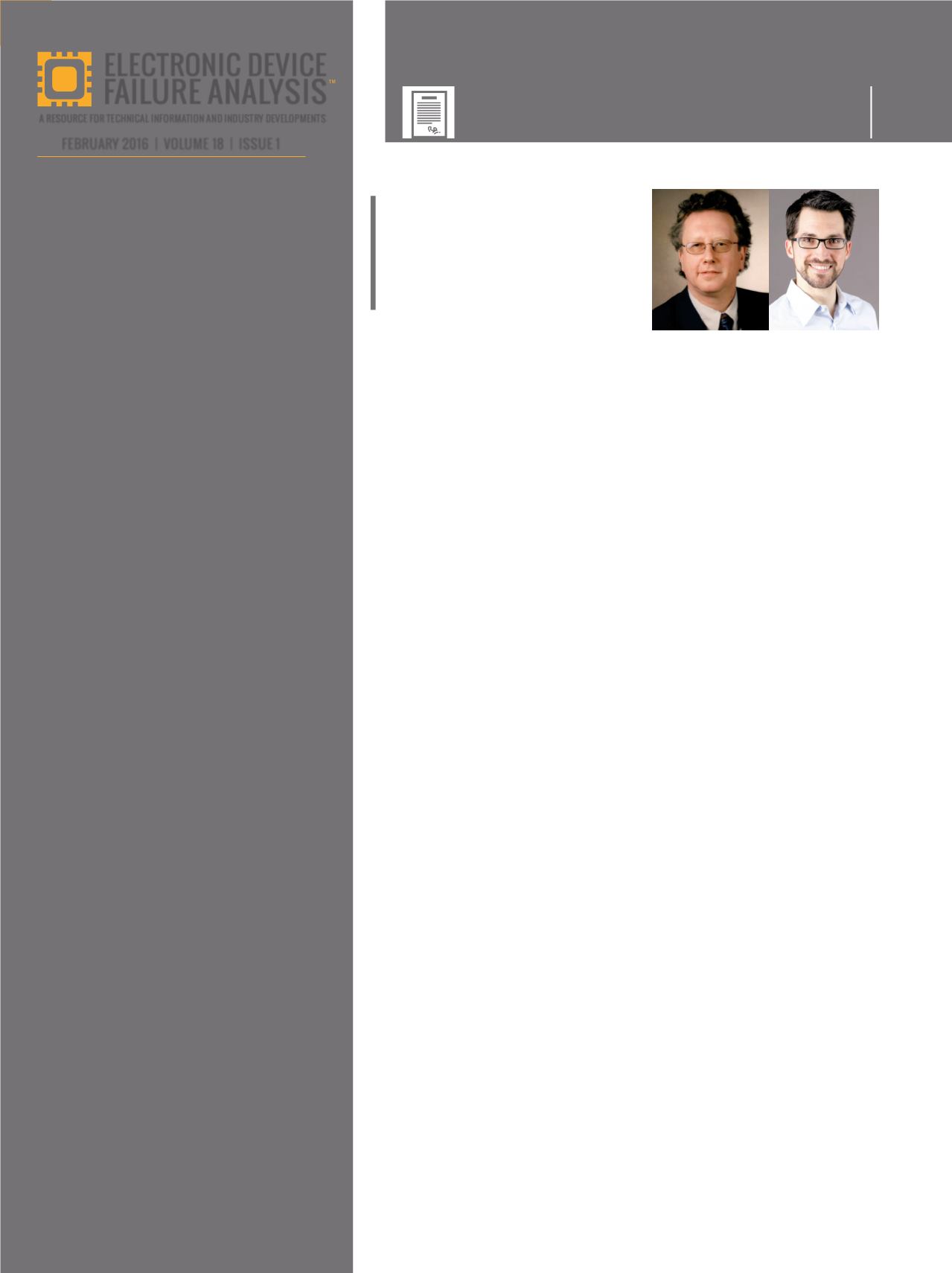
Christian Boit and Philipp Scholz
TUB University of Technology
Berlin, Germany
christian.boit@tu-berlin.de philipp. scholz@tu-berlin.de