


 6 / 62

 edfas.org
ELECTRONIC DEVICE FAILURE ANALYSIS | VOLUME 18 NO. 1
6
Table 2 Experimental study of Si-CCD and InGaAs camera detection capability
Voltage/current applied
Si-CCD camera detection
InGaAs camera detection
1 V/5.5 µA
No defect detected
1.1 V/6.24 µA
1.2 V/6.95 µA
1.3 V/7.68 µA
1.4 V/8.14 µA
1.5 V/9.13 µA
1.6 V/9.87 µA
1.7 V/10.63 µA
1.8 V/11.38 µA
1.9 V/12.14 µA
2 V/12.91 µA
Defect detected
2.1 V/13.69 µA
2.2 V/14.47 µA
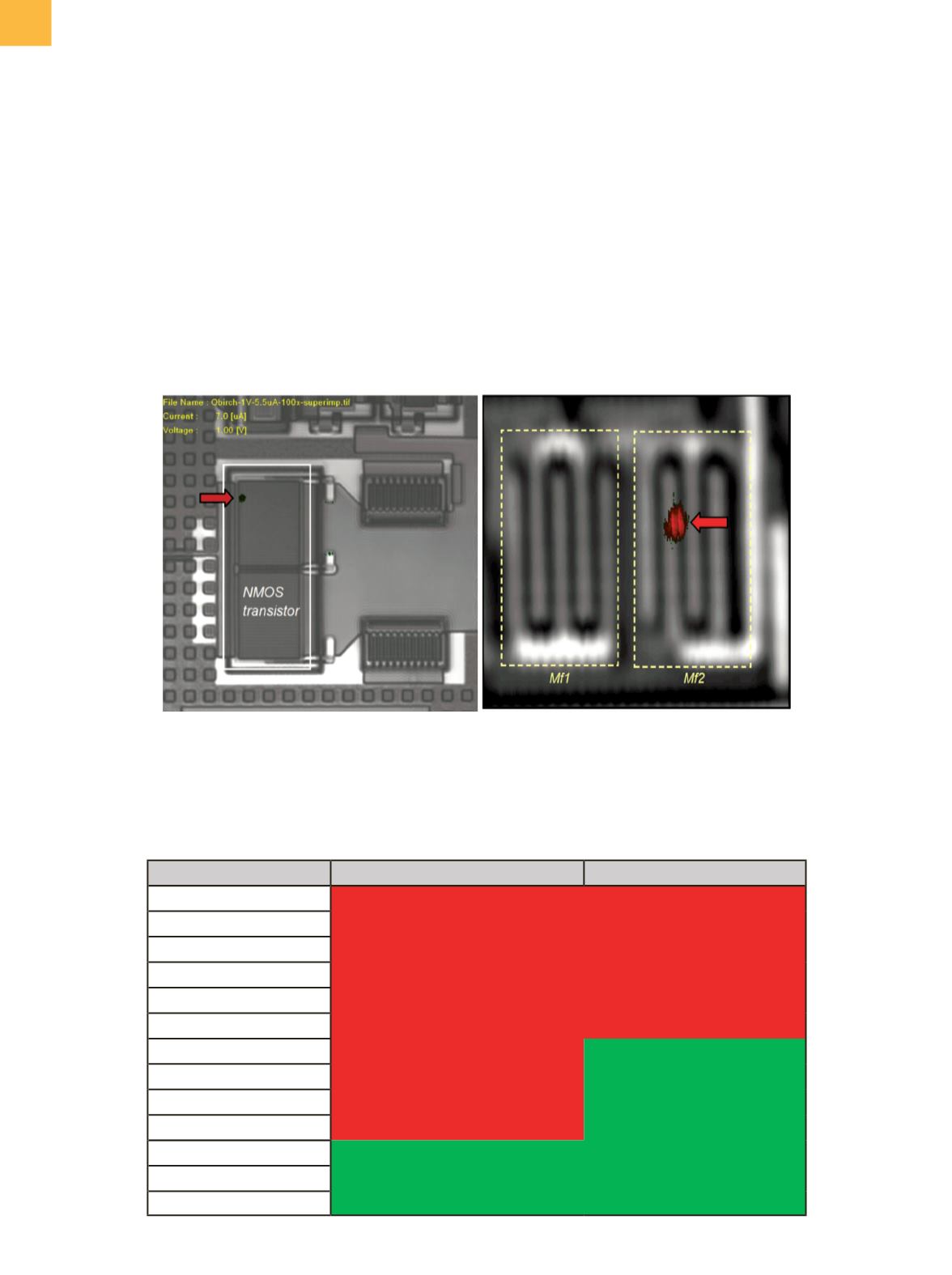
Fig. 2
(a) TLS localization in case 1, within the ESD structure, based on NMOS device. (b) TLS overlay with pattern showing the
OBIRCH signature observed on Mf2 NMOS device by microprobing
(a)
(b)
time for the Si-CCD camera was approximately a few
minutes, but for a voltage below 1.6 V, the integration
time for the InGaAs camera was approximately 30 s (Fig.
3a). The hotspot was visible starting at 1.6 V for the InGaAs
camera and at 2 V for the Si-CCD camera (Fig. 3b), confirm-
ing Planck’s radiation lawdepends onwavelength camera
sensitivity (explained in Ref 6). This experiment confirms
that bothemission cameras are suitable for silicondefects,
with no difference in terms of spectrumemission but with
higher sensitivity for the InGaAs camera. When compared
to TLS, it is an alternative to photoemission, and TLS has
the advantage of selecting the failing path and injecting
voltage or current by microprobing.
ATOMIC FORCE PROBING
Atomic force probingmeasurementswere done in case
2, where the Mf2 NMOS transistor was found to be leaky.
This NMOS transistor comprises four fingers. By measur-
ing the subthreshold current of each finger (measurement
done by increasing and decreasing the voltage), it was
observed that three of the four fingers were leaky (Fig. 4).
Finger 3 hadnormal leakage andwas locatedbetween two
leaky fingers. Despite identifying three leaky fingers, the
OBIRCH signature pinpointed the defect only on finger 2.
This interesting result was confirmed in other parts, sug-
gesting that the TLS or emission techniques revealed only