


 8 / 62

 edfas.org
ELECTRONIC DEVICE FAILURE ANALYSIS | VOLUME 18 NO. 1
8
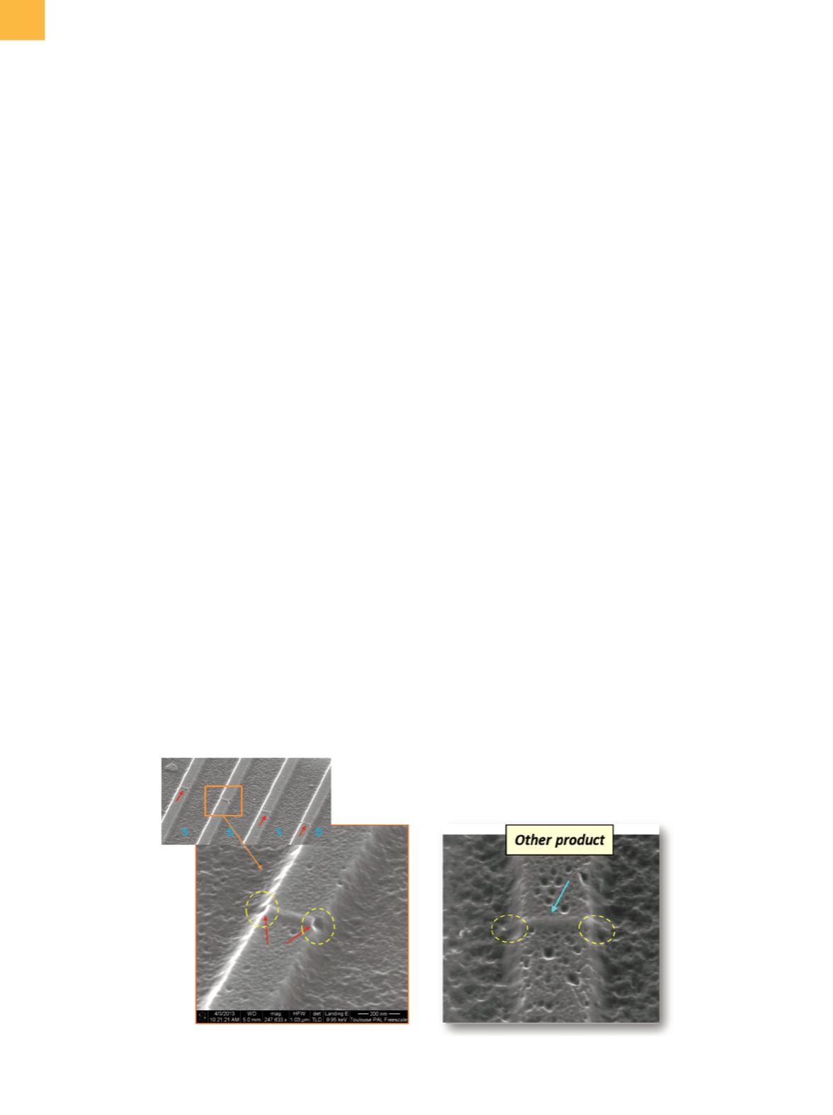
Fig. 6
Tilted SEM image after Wright etch delineation on different product
hairline is suspected to be unexpected
n
-doped silicon at
the surface of the
p
-doped channel. The PVC images were
obtained using high-resolution SEM with sample tilt and
beamdecelerationmode (consisting of the application of
a positive voltage to the sample holder). This configura-
tion is highly recommended to detect pipeline defects by
improving the collection of secondary electrons.
SILICON CRYSTALLINE DELINEATION ETCH
To verify the PVC contrast at the silicon substrate level,
a silicon delineation etchwas performedwithWright etch
solution;
[8]
the
p
-type etch rate is higher than the
n
-type
area etch rate
[9]
with this delineation etch. After etching
with Wright solution for 2 s, the failing NMOS device was
inspected with an SEM; a bump was observed at the
dark line location previously observed on the PVC image
(Fig. 6). This topographic anomaly is consistent with the
hypothesis of an abnormal presence of an
n
-type area in
the NMOS channel (
p
-doped). This unexpected
n
-doped
area crossing the whole channel width explained the
NMOS source-to-drain leakage. In addition to its dopant
delineation capability, Wright etch is also widely used to
delineate silicon crystalline defects, creating typical etch
pit signatures. Those etch pits were observed at the edges
of the abnormal silicon bump and revealed the dopant
anomaly associated with a crystalline defect
[2]
(circled in
yellow in Fig. 6). To confirm and better understand this
complex defect, more investigationswere performedwith
advanced FA techniques.
AFM/SMM TECHNIQUE
Apart fromcase 2was selected to continue the analysis
on the pipeline signature. Surface topography measure-
ments using AFM did not reveal a conclusive anomaly at
the silicon level (Fig. 7). However, SMM analysis showed
an anomalous line contrast in the dC/dV response image,
which typically provides information about the doping
levels. The dark lines observed through the channels of
Mf2 (red arrows in Fig. 7) indicate an unexpected doping
response in the channel active area. These results were
consistent with physical delineation etches that gave
similar pipeline results (see Fig. 6 from the part in case 1).
In contrast, the same techniquewas applied on the failing
device in case 3, where silicon dislocations were found by
physical delineation etch and TEM analysis (refer to the
next section). In this case, SMM was not able to highlight
a defect signature (Fig. 8); this suggested that the nature
of the defect is different. Presumably, the threshold con-
ductivity of free carriers is not in the detection range of
SMM as compared to a pipeline defect, even if the defect
is considered to be conducting.
PLANAR TEM ANALYSIS
Based on previous findings, TEM characterization
was required. Planar TEM samples were prepared on the
defective parts of each product. In case 2 (with pipeline),
TEM images showed crystallographic defects in active
areas, at the vicinity of the anomalous lines observed
during SMM analysis (Fig. 9). The crystalline defects were
noncontinuous lines that were only localized in gate areas.
The defects were perpendicular to source-drain fingers
and appeared to be very close to the surface. Also, con-
tinuous lines were observed in the trench area (shallow
trench isolation), nearly in the extension of the discon-
tinuous lines (far left in Fig. 9). In this case, it was found
to be a pipeline defect in the active area. In case 3, TEM
images also showed crystallographic defects in the active
areas. However, the defects were long, continuous lines