


 5 / 62

 edfas.org
5
ELECTRONIC DEVICE FAILURE ANALYSIS | VOLUME 18 NO. 1
Table 1 Summary of investigations performed on the various products studied
Case 1
Case 2
Case 3
Failure mode
Parametric leakage
Electrical functional
Parametric leakage
Defect signature
Pipeline defect
Pipeline defect
Silicon dislocation
Impacted device type
NMOS
NMOS
NMOS
FA
techniques
TLS
X
X
…
Photoemission
X
…
X
AFP
…
X
…
PVC
X
…
…
Silicon delineation etch
X
X
…
SCM/SMM
…
X
X
Planar TEM
…
X
X
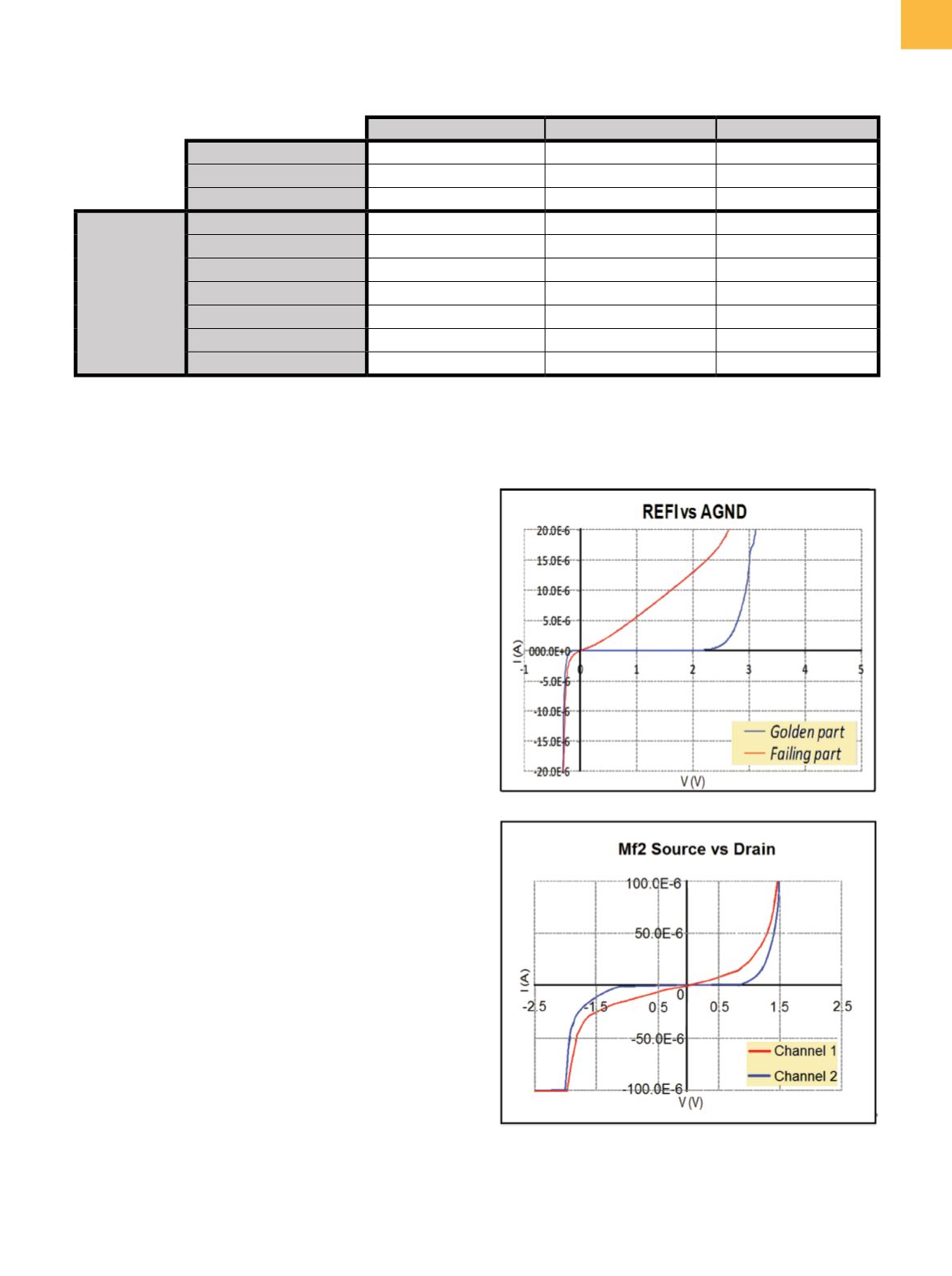
Fig. 1
(a) Parametric leakage characteristic of case 1. (b)
Functional failure. Leakage found bymicroprobing on
failing Mf2 NMOS device in case 2
(a)
(b)
(ESD) structures and single embedded analog transistors
inside a block circuit. The commonality in the three cases
is that the defective device type is always the same: an
NMOS structure.
All the products presented failed at ambient tem-
perature. In case 1, the failurewas observed between two
external pins, REFI and GND, with a leakage of approxi-
mately 2.6 µA at 2 V, compared to a few nanoamps on a
“good” part (Fig. 1a). In case 2, the failure was due to an
offset of 30 mV on the current-sensing circuit of channel
2, generating a functional failure. Microprobing analysis
demonstrated that the failure was due to a drain-source
leakage of the Mf2 (used in the current-measuring chain)
NMOS transistor within the output comparator circuit (Fig.
1b). Based on those results, case 1 was opened from the
backside, and the silicon substrate was thinned.
Thermal laser stimulation was carried out by apply-
ing 1 V between REFI and GND. In this case, the position
of the optical beam induced resistance change (OBIRCH)
spot was located within the ESD structure of the pad and
especially in a specific area of the NMOS transistor (Fig.
2a). TLSwas applied fromthe frontside in case 2, between
the source and drain of this NMOS (Mf2 transistor). The
OBIRCH signature was located on one of the four NMOS
fingers (Fig. 2b). Inboth cases, theOBIRCHsignatureswere
located on the NMOS transistor.
COMPARATIVE STUDY: EMMI/
OBIRCH/InGaAs CAMERA
Anexperimental studywas done in case 1. Leakagewas
initially detected by using TLS (1 V/7 µA/integration time
= 10 s). The aimof this study was to understandwhat type
of defect canbe detectedby the cameras and todetermine
the detection threshold of silicon charge coupled device
(Si-CCD) or InGaAs cameras. The voltage/current was then
increased until the camera could detect the emission of
photons (Table 2). For a voltage below 2 V, the integration