
iTSSe
TSS
A D V A N C E D M A T E R I A L S & P R O C E S S E S | N O V E M B E R / D E C E M B E R 2 0 1 6
4 2
iTSSe
TSS
FEATURE ARTICLE
10
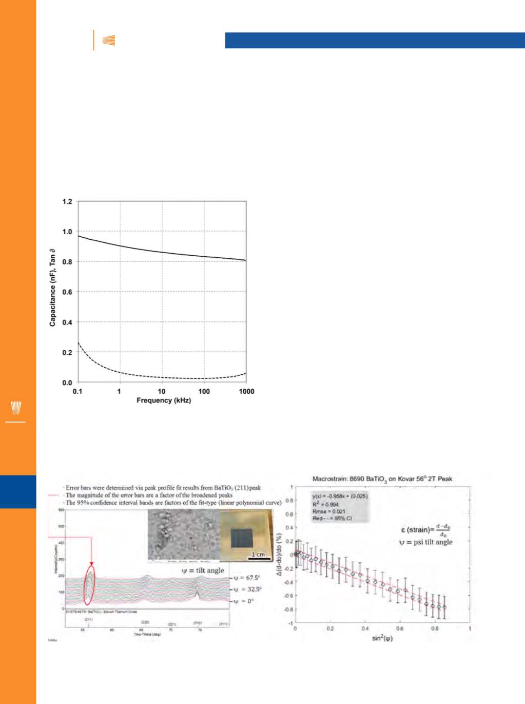
Fig. 3 —
Frequency dependent capacitance and dielectric loss
(tan ∂) of 4 mm
2
capacitors defined on as sprayed 5-7 µm thick films
on Kovar. Low frequency dielectric loss is a common attribute of
as-sprayed BaTiO
3
that exhibits significant space charge contribu-
tion to total polarization.
Fig. 4 —
XRDmeasurement and strain calculation on the 4 µm thick BaTiO
3
film on Kovar substrate. The strain was on the order of ~1%, corre-
sponding to ~1 GPa residual compressive in-plane stress.
low melting point substrates such as glass, metal, or plastic.
Moreover, BaTiO
3
is susceptible to point defect formation by
highly reducing thermal processes. Thermal spray lends itself
to electron-rich point defect formation due to volatilization
of typical A-site substitution cations, including bismuth or
lead. In addition, oxygen vacancy formation that contributes
to sub-band electrical transport is enhanced by the thermal
processing and rapid quenching used in thermal spray pro-
cesses. The associated dielectric properties, such as insulation
resistance, dielectric constant, and dielectric loss are therefore
significantly impacted by melting/solidification in traditional
plasma spray.
The AD process was used to successfully integrate high
density thick BaTiO
3
films with copper (Tm = 1085°C) at room
temperature. The aerosol deposited BaTiO
3
film crystal struc-
ture, grain size, residual strain, and dielectric properties are
currently being investigated. Preliminary results show that
5-7 µm thick BaTiO
3
films produce 1 nF capacitors with a 2 x
2 mm (providing a 4 mm
2
area) gold electrode. A 3 x 3 matrix
of electrodes was defined on the 1-cm deposition area. Each
electrode spans a 4 mm
2
area. Seven of the nine 4 mm
2
elec-
trodes demonstrate potential as capacitors with loss values in-
dicative of continuous, non-cracked films. Figure 3 shows the
frequency dependent capacitance and dielectric loss from100
Hz to 1 MHz. As-aerosol-deposited films exhibit some space
charge contribution to polarization. The permittivity of the
films was calculated to be k~200, which is consistent with oth-
er published research.
Although polycrystalline BaTiO
3
capacitors generally
exhibit k>1000 at room temperature, these films exhibit sig-
nificant crystalline disorder and amorphous grain boundary
volume. This combination of grain boundary volume and
crystalline disorder reduces polarization by hindering Ti4+
mobility within the unit cell and reduces domain wall motion
by defect pinning. In addition, these films exhibit significant
in-plane crystallographic strain quantified by XRD analysis.
The in-plane strain is approximately 1%as determined by XRD
analysis (Fig. 4), which corresponds to an approximate com-
pressive stress of 1 GPa.
The as-deposited coatings also have very small grain
size (20-75 nm or less). Small grain size may be beneficial for
structural ceramics, but larger grain size on the order of


