
iTSSe
TSS
A D V A N C E D
M A T E R I A L S
&
P R O C E S S E S |
N O V E M B E R / D E C E M B E R
2 0 1 6
4 1
iTSSe
TSS
FEATURE ARTICLE
9
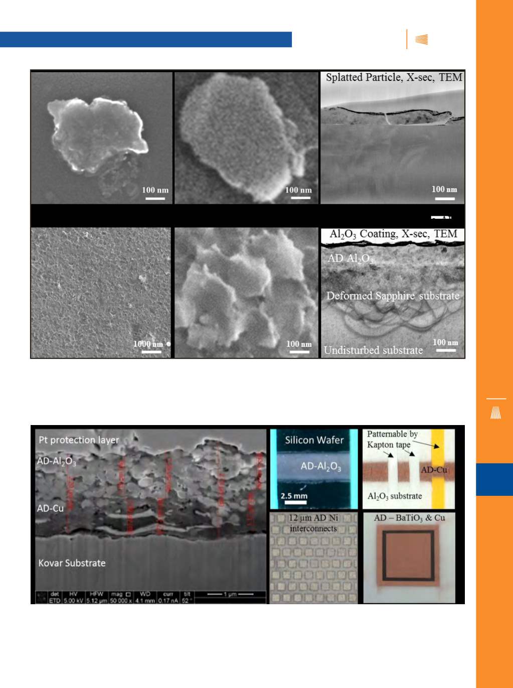
Fig. 1 —
(Top row) SEM top view images of splatted Al
2
O
3
particles from quasi-static loading (left) in the indentation experiment and impacting
on the substrate in the AD process (middle). Cross-section TEM image of AD splatted particle showing nanocrystallinity (right). (Bottom row)
SEM top view images of AD Al
2
O
3
films at low (left) and high (middle) magnifications. Cross-section TEM image of AD Al
2
O
3
coating on sapphire
shows nanocrystallinity and deformed substrate (right).
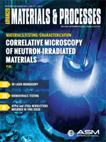
Fig. 2 —
Examples of integrated AD coatings—Al
2
O
3
-Cu graded coating on Kovar, Al
2
O
3
on Si, Cu on alumina, patterned Ni interconnect on
alumina, and Cu-BaTiO
3
-Cu on alumina.


