


 17 / 62

A D V A N C E D
M A T E R I A L S
&
P R O C E S S E S | F E B R U A R Y
2 0 1 6
1 7
FEI Co., Hillsboro, Ore., by improving
the speed and reliability of its Dual-
Beam instrument. Fraunhofer CAM has
been closely involved in many of those
developments.
S/TEM IMAGING
AND ANALYSIS
Recent developments in S/TEM
have greatly increased its utility in semi-
conductor applications. The advent of
practical image correctors has great-
ly simplified interpretation of high-
resolution TEM images. Similarly, probe
correctors have improved the lateral
resolution of imaging and composition-
al analysis by reducing the size of the
scanned STEM “spot.” Improvements
in electron source technology and in-
corporation of monochromators have
improved both TEM imaging and STEM
probe diameter by reducing the adverse
effects of chromatic aberration. This is
particularly important at lower beam
energies used to image light materials
and reduce knock-on damage. Using a
highly efficient multi-detector energy
dispersive x-ray spectrometer, a mono-
chromated, probe-corrected STEM can
deliver maps of elemental distribution
with atomic scale resolution.
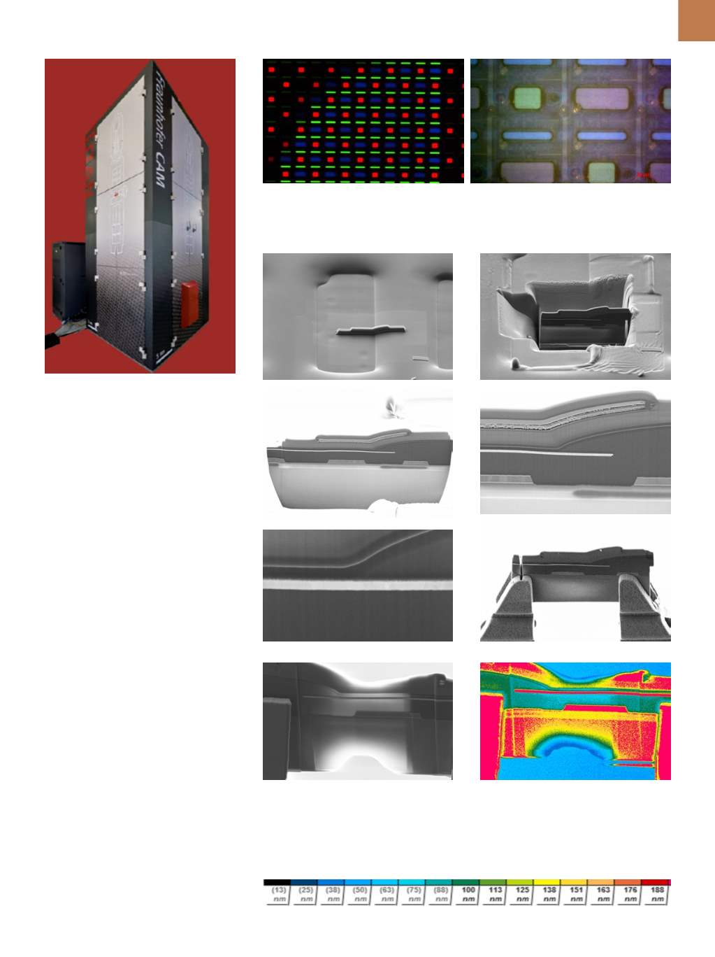
Fig. 1 —
FEI Titan G2 60-300.
Fig. 2 —
(a) Magnified view of an operating Super AMOLED display from a Samsung Galaxy
III smart phone; (b) higher magnification view of powered down display acquired with a light
microscope.
Fig. 3 —
DualBeam TEM sample preparation workflow: (a) Protective layers deposited at loca-
tion of section to protect upper layers from erosion; (b) FIBmilling leaves thick section ready for
extraction; (c) section surface; (d) higher magnification of section surface; (e) still higher magni-
fication of region of interest at edge of blue pixel; (f) extracted section transferred to TEM holder;
(g) section after final thinning; (h) final thickness map based on backscattered electron signal:
(a)
(b)
(a)
(b)
(c)
(d)
(e)
(f)
(g)
(h)