


 22 / 82

A D V A N C E D M A T E R I A L S & P R O C E S S E S | N O V E M B E R / D E C E M B E R 2 0 1 6
2 2
L
aser scanning confocal micros-
copy (Fig. 1) provides non-contact,
nanometer level profile (depth)
resolution to measure surface rough-
ness and film thickness data on a vari-
ety of materials and components. This,
along with the possibility of high resolu-
tion and large area mapping, are lead-
ing to new opportunities for materials
characterization.
To measure surface profiles, tra-
ditional contact methods risk surface
damage, particularly for soft materials.
Additionally, surface changes smaller
than the stylus tip cannot be measured
or quantified. A laser microscope can be
used on soft and hard materials alike
because it is non-contact and the laser
beam diameter is much smaller than a
stylus, which provides more accurate
data. The laser also makes it easier to
measure surfaces on an entire area
without the need to properly place a
measuring device (Fig. 2).
Scanning electron microscopy
(SEM) is typically used when resolution
beyond optical microscopy is required.
A key advantage of laser microscopy
compared to SEM is that high resolu-
tion images (with magnifications up
to 28,000×) are possible in air with-
out additional surface preparation.
This makes laser microscopy a faster
option for imaging materials and com-
ponents. With an automated stage and
image stitching capabilities, large-area
high-resolution images can be obtained
ADVANTAGESOF 3D LASER
SCANNINGCONFOCAL
MICROSCOPY
3D laser microscopy is opening new areas of study for metallic
alloys and coatings in power generation applications.
John Shingledecker,* John Siefert, and Daniel Purdy,* Electric Power Research Institute, Charlotte, N.C.
Jonathan Tedesco and Andrew Szafarczyk, Keyence Corp., Itasca, Ill.
*Member of ASM International
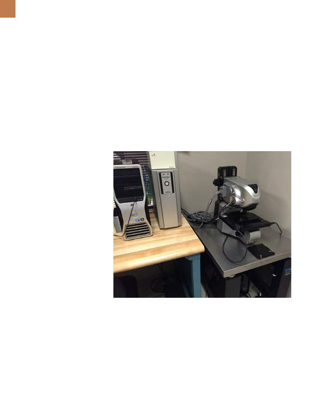
Fig. 1 —
Keyence VK-X laser microscope.
while retaining spatial distances and
associated 3D depth information,
which is not possible with a SEM.
Laser microscopy is used in a vari-
ety of industries. The ability to measure
depth and soft/optical materials in a
non-contact manner is particularly well
suited for the electronics industry and
chemical industries including a wide
range of applications in CCD micro-
lens characterization, MEMs measure-
ments and failure investigations, silicon
wafer roughness, and film thickness
characterization of transparent mate-
rials such as glasses and lenses. Laser
microscopy is also widely used for met-
als characterization, specifically surface
roughness. In addition, the unique attri-
butes of the laser microscope have led to
expanded characterization applications
for materials in power generation equip-
ment in recent years.
CASE STUDIES
At the Electric Power Research
Institute’s (EPRI) laboratories in Char-