


 20 / 62

2 0
A D V A N C E D M A T E R I A L S & P R O C E S S E S | J U N E 2 0 1 5
as a gate) defined before transducer
scanning begins. Because the acoustic
velocity of the material or materials is
known, the elapsed time of an echo’s
travel from an interface within the gate
can be converted into distance. The pre-
cise depth of the echo at each location
can thus be known by using a program
called the
time difference mode
—and
the range of depths can be displayed by
a sequence of pixel colors.
Figure 3a shows a time differ-
ence acoustic image of the area of one
warped ceramic raft in an IGBT module.
The image was gated to include the sol-
der layer and top surface of the raft be-
neath the solder. The transducer pulsed
ultrasound into themodule frombelow,
and the time difference mode mapped
the surface of the warped raft. Where
the raft surface is highest, the solder is
thinnest. A 2D side view image through
this IGBT module would look some-
thing like the diagram in Fig. 4, where
solder thickness varies. In the diagram,
black items indicate voids in the solder.
In Fig. 3a, solder is thickest (and
raft surface lowest) in the magenta re-
gion near the lower right corner. Solder
is thinnest (and raft surface highest) in
the small red region at the upper left.
Tilting and warping of the raft dimin-
ishes its heat-flow uniformity. In some
IGBT modules, the raft is warped rather
than simply tilted.
The red features away from the
upper left corner indicate voids in the
solder. In both the ceramic raft and
voids, red areas identify items in con-
tact with the heat sink through which
the ultrasound was pulsed. Each void
blocks heat flow and, collectively, may
reduce flow to critical and undesirable
levels.
Figure 3b uses colors to identify
the local depth range of the solder.
During inspection, this type of map
makes it easier to pinpoint unaccept-
able solder thickness. The same tech-
nology is used to examine internal
material interfaces in a much different
application—manufacturing polycrys-
talline diamond (PCD) material for use
in cutting tools such as oilfield drill bits.
The material is made by sintering
a layer of PCD on top of a tungsten car-
bide layer. The tungsten carbide (WC)
makes the tool stronger and adds to its
footprint, making it easier to mount.
These sintered layers form a wafer that
can be cut into individual tool bits, with
the top PCD layer used to perform the
actual cutting.
The desirable outcome of sinter-
ing is a wafer with a uniformly thick lay-
er of PCD on top. Such a wafer, whose
layers are shown in Fig. 5, can be elec-
tromechanically sliced into the max-
imum number of tool bits for a given
application. Wafer price depends on
the number of good tool bits that can
be cut from it. Tool bits where the PCD
layer varies as little as possible from the
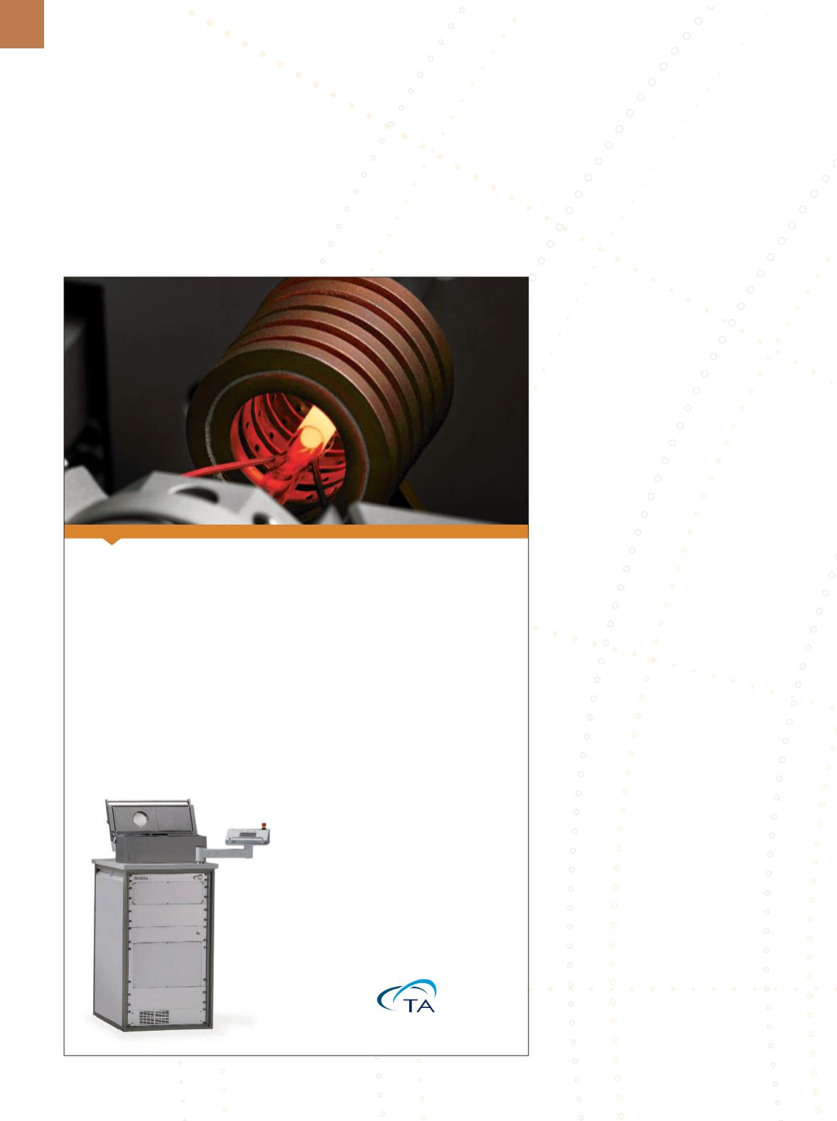
Discover More Steel Research Capability www.tainstruments.com DIL 805 Quenching and Deformation Dilatometer The DIL 805-series quenching and deformation dilatometers provide the most accurate measurements over the widest range of heating, cooling,anddeformationconditions,allowingforthemostsophisticated characterization and optimization of steel processing conditions. The DIL 805 provides critical data for the construction of time-temperature- transformation (TTT) , continuous-cooling-transformation (CCT) , and time-temperature-transformation after deformation (DTTT) diagrams as well as stress-strain curves. Powerful inductive heating and an innovative helium quench system enable heating rates up to 4000 K/s and quenching rates as high as 2500 K/s to capture the extremes of modern processing conditions.