


 19 / 62

1 9
A D V A N C E D
M A T E R I A L S
&
P R O C E S S E S | J U N E
2 0 1 5
A
coustic microscopes pulse ultra-
sound into a sample and use the
return echoes to find and image
cracks, delaminations, and other gap-
type flaws in manufactured parts and
products. New developments in micro-
scope technology, such as those taking
place at Sonoscan Inc., enable mapping
of the point-by-point contour of tilted or
warped interfaces, as well as individual
material layer thicknesses.
If all layers are flat and parallel to
each other, the acoustic image map of
any internal interface will contain uni-
form color pixels because they are all
the same distance from the scanning
ultrasonic transducer. However, an as-
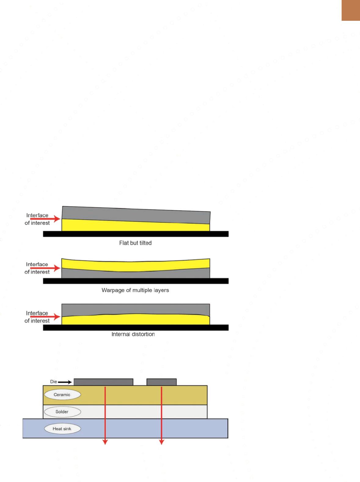
sembly may contain interfaces that are
tilted or warped, as shown in Fig. 1. In
some instances, both warped
and
tilt-
ed interfaces are present in the same
assembly.
In many applications, design con-
straints require these buried layers to
be flat, horizontal, and of uniform thick-
ness, although acoustic imaging may
show different internal geometry. For
example, power insulated gate bipolar
transistor (IGBT) modules often strug-
gle with buried layers. Fast-switching
IGBT modules are frequently used to
handle heavy loads in critical applica-
tions such as railroad engines, heavy
mining equipment, and electric auto-
mobiles. Due to high current levels, the
silicon die that actually performs the
switching must disperse large amounts
of heat.
IGBTmodules are designed so that
heat flows downward through ceramic
plates called
rafts
to a metal heat sink
that dissipates heat into the surround-
ing air (Fig. 2). If the heat sink, raft, and
die are all horizontal and parallel, and
if there are no voids (air bubbles) or
other gaps in the solder bond, heat will
flow downward (arrows in Fig. 1) at the
designated rate. However, if voids are
present or the raft (and perhaps the die
itself) are tilted, heat flow will not meet
specifications, likely causing the die to
overheat and fail electrically.
Acoustic microscopes can image
internal material interfaces fairly quick-
ly because the transducer that pulses
the ultrasound and receives the echoes
from the internal features moves later-
ally at speeds that can exceed 1 m/s.
In addition, the speed of ultrasound
through production materials such as
metals, ceramics, and polymers is typi-
cally measured in thousands of m/s.
Because most sample thicknesses
are measured in millimeters, the pulse
is launched and echoes are received in a
fewmillionths of a second. Consequent-
ly, the moving transducer can receive
echoes from thousands of locations per
second as it scans. Echoes may come
from a solid-to-solid material interface,
or in the case of gap-type defects, a
solid-to-gas (e.g., air) material inter-
face. Each location contributes one pix-
el to the sample’s acoustic image.
IGBT modules are imaged by scan-
ning the transducer, which is inverted,
across the surface of the metal heat
sink at the bottom of the assembly.
Because the transducer’s ultrasound
needs to be coupled to the surface, con-
tact is maintained by a water plume. At
each location, the return echo’s ampli-
tude provides information about the
two materials at the interface. Solid-to-
solid interfaces tend to have lower am-
plitude echoes. Solid-to-gas interfaces
reflect virtually 100% of the ultrasound
and thus produce much higher ampli-
tude echoes that become bright white
pixels in the acoustic image. While
imaging the depth in a sample where
two solid materials are supposed to be
joined, there should be no white areas
indicating voids, delaminations, or oth-
er gaps.
The elapsed time from pulse
launch to echo return is also measured
and recorded. This indicates that the
image comes from within the vertical
extent of the depth of interest (known
Fig. 1 —
Three major types of internal nonplanarity.
Fig. 2 —
Arrows show desired path of heat dissipation from an IGBT module.