


 21 / 62

2 1
A D V A N C E D
M A T E R I A L S
&
P R O C E S S E S | J U N E
2 0 1 5
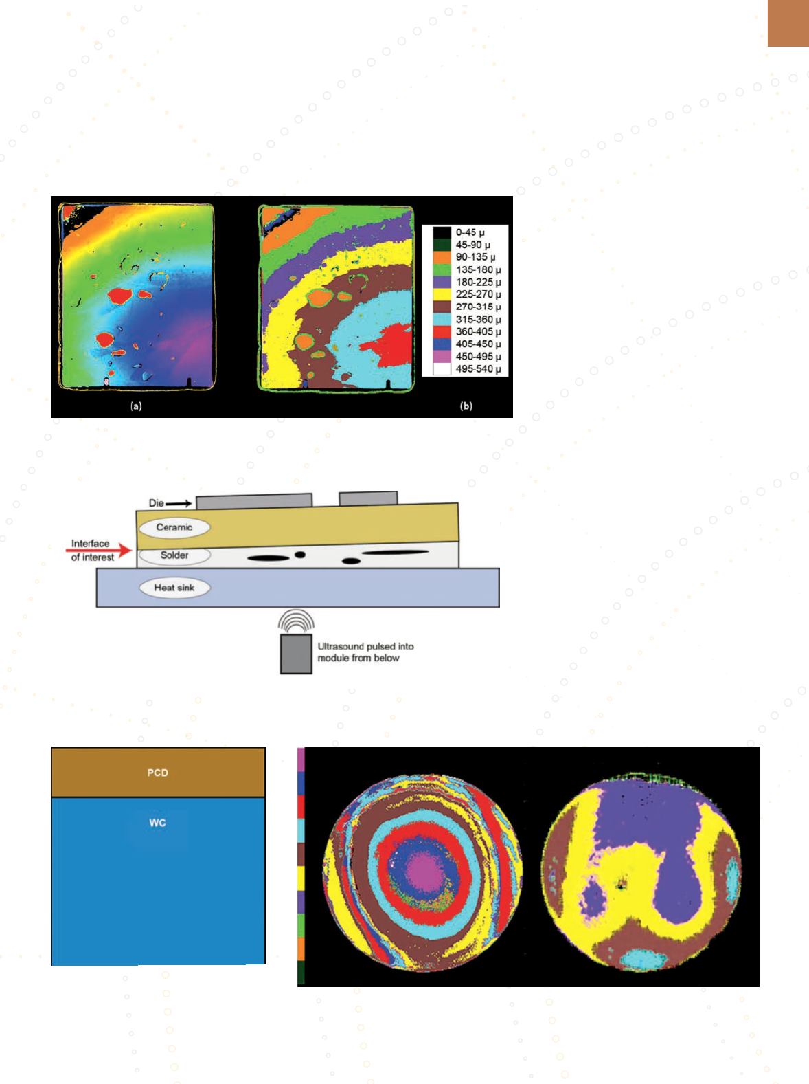
Fig. 3 —
Time difference mode image of solder thickness in IGBT module with a tilted raft (a).
Scale indicates solder thickness (b).
Fig. 4 —
Diagrammatic side view of a module with a tilted raft.
Fig. 5 —
Side view diagram of a portion of
an ideal polycrystalline diamond/tungsten
carbide wafer.
Fig. 6 —
Time difference mode images of two wafers exhibiting extreme variation in PCD thick-
ness (left), andmuch less variation with far more usable area (right).
the brown and pale blue regions on the
two wafers.
The left wafer features many obvi-
ous variations in PCD thickness over
short distances. Over the whole wafer,
PCD thickness ranges from about
0.45 mm to 0.80 mm. The thickest region
is near the center, represented by the
magenta color. The result is that only a
small portion of this wafer is usable.
In contrast, the wafer on the right fea-
tures a total PCD thickness variation of
just 0.20 mm, offering a significantly
larger area to be sliced into tool bits.
In both the IGBT sample and the
diamond sample discussed here, one
face of the buried layer is flat and hor-
izontal—i.e., the top of the PCD wafer,
and the top of the IGBT module’s solder
where it interfaces with the rigid metal
heat sink. If a buried layer were distort-
ed on both of its surfaces, this acoustic
method could image both of the buried
layer’s surfaces in separate images and
map the thickness of the distorted bur-
ied layer.
~AM&P
For more information:
Tom Adams is
a consultant for Sonoscan Inc., 2149 E.
Pratt Blvd., Elk Grove Village, IL 60007,
847.437.6400,
info@sonoscan.com,
www.sonoscan.com.
ideal thickness are desirable because
any cutting tool breakdown requires an
expensive and time-consuming repair.
Imaging wafers acoustically pro-
duces a map showing the local depth of
the interface between the PCD and WC,
i.e., the PCD thickness. Figure 6 shows
the acoustic images of two 55-mm wa-
fers. Each color represents a vertical
extent of 0.05 mm. The ideal thickness
for this application is roughly 0.60 mm,
represented by the boundary between