


 17 / 62

A D V A N C E D
M A T E R I A L S
&
P R O C E S S E S | J U N E
2 0 1 5
1 7
NANOTECHNOLOGY
BRIEFS
Aleris, Cleveland, offers a new 7017 aluminum alloy in North America for commercial plate and defense
uses. After extensive review and testing, the U.S. Army Research Lab issued MIL-DTL-32505 for use in armor
applications. 7017 offers high strength, good weldability, and corrosion resistance. It is currently used in
Europe and Asia on combat vehicles to achieve superior ballistic protection.
aleris.com.
NEW WAY TO GROW METAL
NANOSTRUCTURES
Michael Tringides, physicist at
the DOE’s Ames Laboratory and pro-
fessor of physics and astronomy at
Iowa State University, saw unusual
atom movement when a few thousand
lead atoms were dropped onto a flat,
smooth lead-on-silicon surface, all
at low temperatures, on an area just
one-twentieth the width of a human
hair. Scientists expected to see “ran-
dom-walk diffusion” with atoms mill-
ing around, appearing to have no idea
where they’re going or that any fellow
atoms are near them. Typically, atoms
eventually run into each other and cre-
ate small structures.
“Instead, we saw atoms very fo-
cused and working together to quick-
ly create tiny lead nanostructures,”
says Tringides. “That kind of
collective
diffusion
is really the exception to the
rule in atom movement. Plus, we were
surprised by how fast well-organized
crystal structures nucleate at such cold
temperatures, where movement is typ-
ically slow.”
This collective, fast diffusion
could represent a new way to grow per-
fect, tiny metal nanostructures. “Un-
derstanding the basic science of how
materials work at these nanoscales
may be key to making nanotransis-
tors, nanoswitches, and nanomagnets
smaller, faster, and more reliably,”
says Tringides.
For more information:
Michael Tringides, 515.294.6439,
mctringi @iastat.edu,
physastro.iastate.edu.GRAPHENE FOR FUTURE
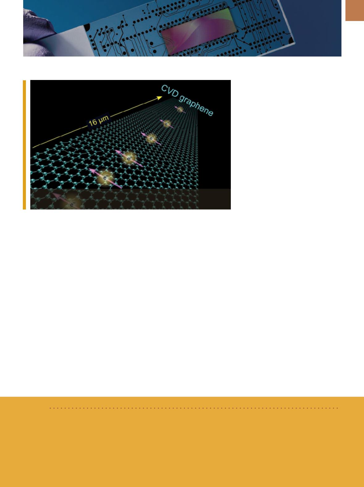
SPINTRONIC DEVICES
Researchers at Chalmers Univer-
sity of Technology, Sweden, discovered
Graphene may enable spintronics to complement traditional electronics. Courtesy of
M. Venkata Kamalakar, et al.
BRIEF
A breakthrough in artific al photosynthesi was achieved through a system that captu es carbon dioxide emissions
before they are vented into he a mosph re and th n, powered by solar ene gy, converts the emissions into valu ble
chemical products, including biodegradable pla ics, p armaceutical drugs, and eve liquid fuels. S ientists with the
DOE’s Lawrence Berkeley Nation l Laboratory,
Calif., nd th
University of California,
B keley,
created a hybrid
system of semiconducting nanowires and bacteria that mimics the natural photosynthetic process. The artificial
system synthesizes the combination of carbon dioxide and water into acetate, the most common building block for
biosynthesis.
lbl.gov,
berkeley.edu.
that large area graphene can preserve
electron spin over an extended peri-
od, and communicate it over greater
distances than previously thought.
This could open the door to spin-
tronics development, with an aim to
build faster and more energy-efficient
memory and processors in computers.
Spintronics is based on the quantum
state of the electrons and the technol-
ogy is already used in advanced hard
drives for data storage and magnetic
random accesses memory. Graphene
is a promising candidate for extend-
ing spintronics use in the electronics
industry. The thin carbon film is not
only an excellent electrical conductor,
but also theoretically has the rare abil-
ity to maintain the electrons with the
spin intact.
Researchers
conducted
their
experiments using CVD graphene,
produced through chemical vapor
deposition (CVD). This method gives
the graphene a lot of wrinkles, rough-
ness, and other defects. But it also
has advantages—there are good pros-
pects for the production of large area
graphene on an industrial scale. CVD
graphene can also be easily removed
from the copper foil on which it grows
and is lifted onto a silicon wafer, which
is the semiconductor industry’s stan-
dard material. Although the quality
of the material is far from perfect,
the group shows parameters of spin
that are up to six times higher than
those previously reported for CVD
graphene on a similar substrate.
www.chalmers.se/en.