


 20 / 50

P. Frigola
RadiaBeam
Technologies LLC
Santa Monica, Calif.
O.A. Harrysson
T.J. Horn
H.A. West*
R.L. Aman
J.M. Rigsbee,
FASM*
Center for Additive
Manufacturing and
Logistics
North Carolina State
University, Raleigh
D.A. Ramirez
L.E. Murr, FASM*
F. Medina
R.B. Wicker
E. Rodriguez
W.M. Keck Center
for 3D Innovation
University of Texas,
El Paso
ADVANCED MATERIALS & PROCESSES •
JULY 2014
20
D
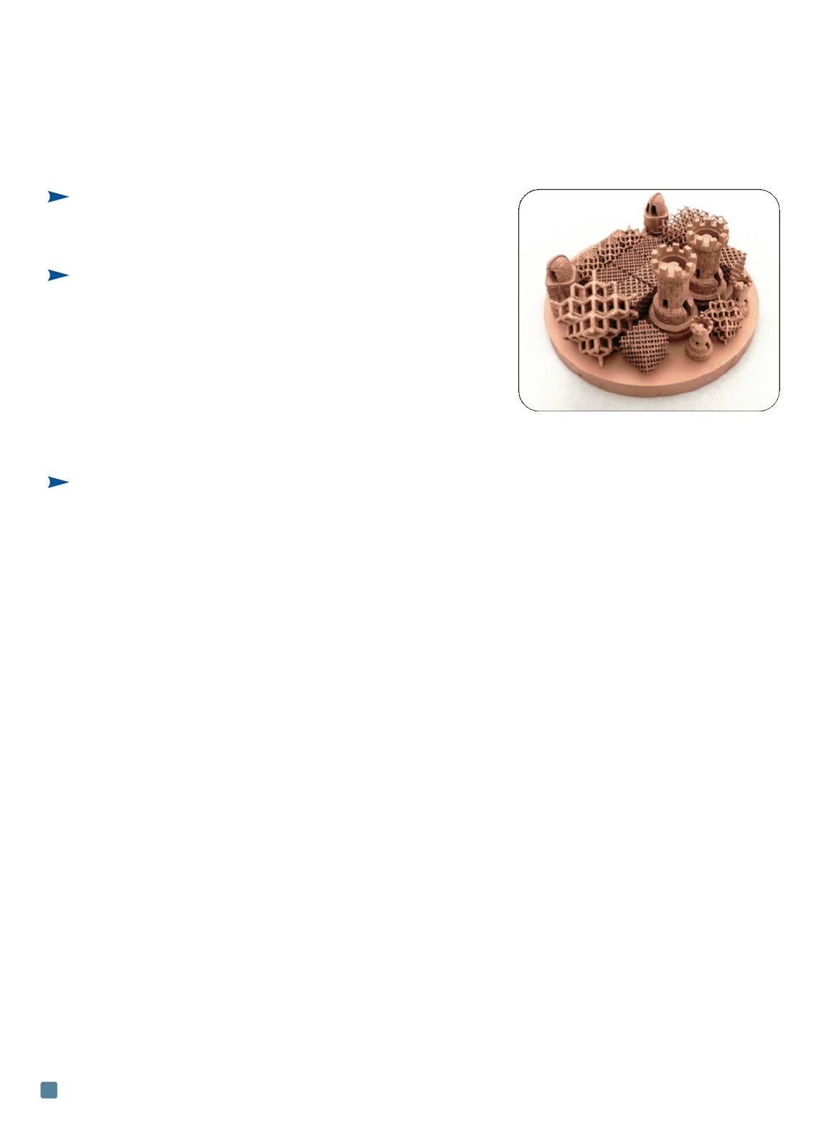
irect fabrication of fully dense metal
structures using the electron beam
melting (EBM) process developed by
Arcam AB, Sweden, has been successfully
demonstrated for a wide range of materials in-
cluding Ti-6Al-4V
[1,11,9]
, cobalt chromium
[7,6]
,
titanium-aluminide
[4,8]
, H-13 steel
[2]
, and nickel-
base alloys
[10]
. A growing interest in additive
manufacturing (AM) to build components
from copper and copper alloys
[5,13,12]
is spurring
a variety of applications including novel radio
frequency (RF) accelerating structures.
A critical issue for high average power,
high brightness photoinjectors—the technol-
ogy of choice for generating high brightness
electron beams used in many of today’s linear
accelerators—is efficient cooling. RadiaBeam
Technologies is exploring the use of AM to
fabricate complex RF photoinjectors with
geometries optimized for thermal manage-
ment: Spatially optimized internal cooling
channels can be fabricated without the con-
straints typically associated with traditional
manufacturing methods.
However, several properties of pure copper
present significant processing challenges for di-
rect metal AM. For one, pure copper has a rela-
tively high thermal conductivity (401
W•m−1•K−1 at 300K) which, while ideal for
thermal management applications, rapidly con-
ducts heat away from the melt area resulting in
local thermal gradients. This can lead to layer
curling, delamination, and ultimately, build and
part failure. Additionally, copper’s high ductility
hinders post-build powder removal and recov-
ery. Particles also tend to agglomerate, reducing
overall flowability and impeding powder deposi-
tion. Because Cu is sensitive to oxidation, great
care must be taken in handling and storage be-
fore, during, and after part fabrication.
Fabrication methods
Initial experiments focused on developing
stable parameters for processing copper using
EBM. An Arcam model S12 at North Carolina
State University, and an Arcam model A2 at the
University of Texas El Paso, fabricated the sam-
ples for these experiments. EBMhardware is de-
scribed elsewhere in detail
[3,4,5,6]
. A circular start
plate made of oxygen free, high conductivity
(OFHC) copper measuring approximately 150 x
10 mm leveled on a 10-mm-thick bed of loose
copper powder was the build substrate. Initially,
the electron beam scans the start plate surface
at high power and high speed, raising the plate
temperature to 500°-600°C. Fast scan rates allow
maintenance of a relatively high temperature
throughout the build process, reducing internal
stresses caused by thermal gradients.
Processing each layer typically requires two
separate parameter steps called
themes,
which
contain all of the required process parameters,
such as beam speed and power, and focus off-
set. The first step is
preheating,
which raises the
powder temperature and causes it to lightly sin-
ter together. This mechanical bond facilitates
the next step,
melting,
which is divided into two
sub-steps:
contours
and
hatching.
The contours
step uses relatively low current and speed to
trace the outline of each layer with a propri-
etary control step called
multi-beam,
which
uses the high scan rate capabilities to jump be-
tween multiple locations on the contour, ap-
proximating multiple beams that are able to
simultaneously maintain multiple (~60) melt
pools. This approach improves surface finish
compared to single-spot contouring while
maintaining productivity. In the hatching step,
beam current and speed are increased and the
beam is rastered to melt the area between con-
tours. With each layer, the hatch direction is ro-
tated 90° and spacing between hatch lines is
offset by 0.05 mm.
EBM process parameters
Preliminary efforts in parameter develop-
ment focused on evaluating and optimizing
powder rawmaterial. Powders from three man-
ufacturers were obtained. Two high-purity
99.99% Cu powders (A and B) were atomized
in argon, while a third low-purity 99.8% Cu
Fabricating Copper Components
with Electron Beam Melting
The ability
to make
components
from copper
and copper
alloys via
additive
manufacturing
is spurring a
range of novel
applications.
*Member of ASM International