


 23 / 50

ADVANCED MATERIALS & PROCESSES •
JULY 2014
23
ponent than in Fig. 3b and the part
temperature was considerably
higher, producing a component
with a more conventional Cu
equiaxed grain structure contain-
ing coherent annealing twins. This
structure does not show any direc-
tionally solidified microstructure.
Table 1 shows initial testing re-
sults of the physical properties.
Bulk thermal conductivity
(W/m*k) measurements were
recorded at ambient conditions
using the ThermTest TPS 2500S
thermal constants analyzer
(ISO/DIS 22007-2.2). Electrical
conductivity (% IACS), also carried
out in ambient conditions, was
measured with a Verimet Eddy
current conductivity meter. Tensile
testing was carried out on ASTM
E8 subsize specimens fabricated in
the
XYZ
and
XZY
orientations per
ASTM F2921.
Prototype fabrication
and field testing
The final step in this feasibility
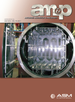
study was to demonstrate the ability to fabricate a complex
geometry that incorporates internal cooling channels. The
block shown in Fig. 4 was fabricated with three different
channel sizes running straight through the part in three or-
thogonal directions that curve through the part with 90°
elbows. This design also demonstrates the ability to clean
sintered powder from internal cooling channels.
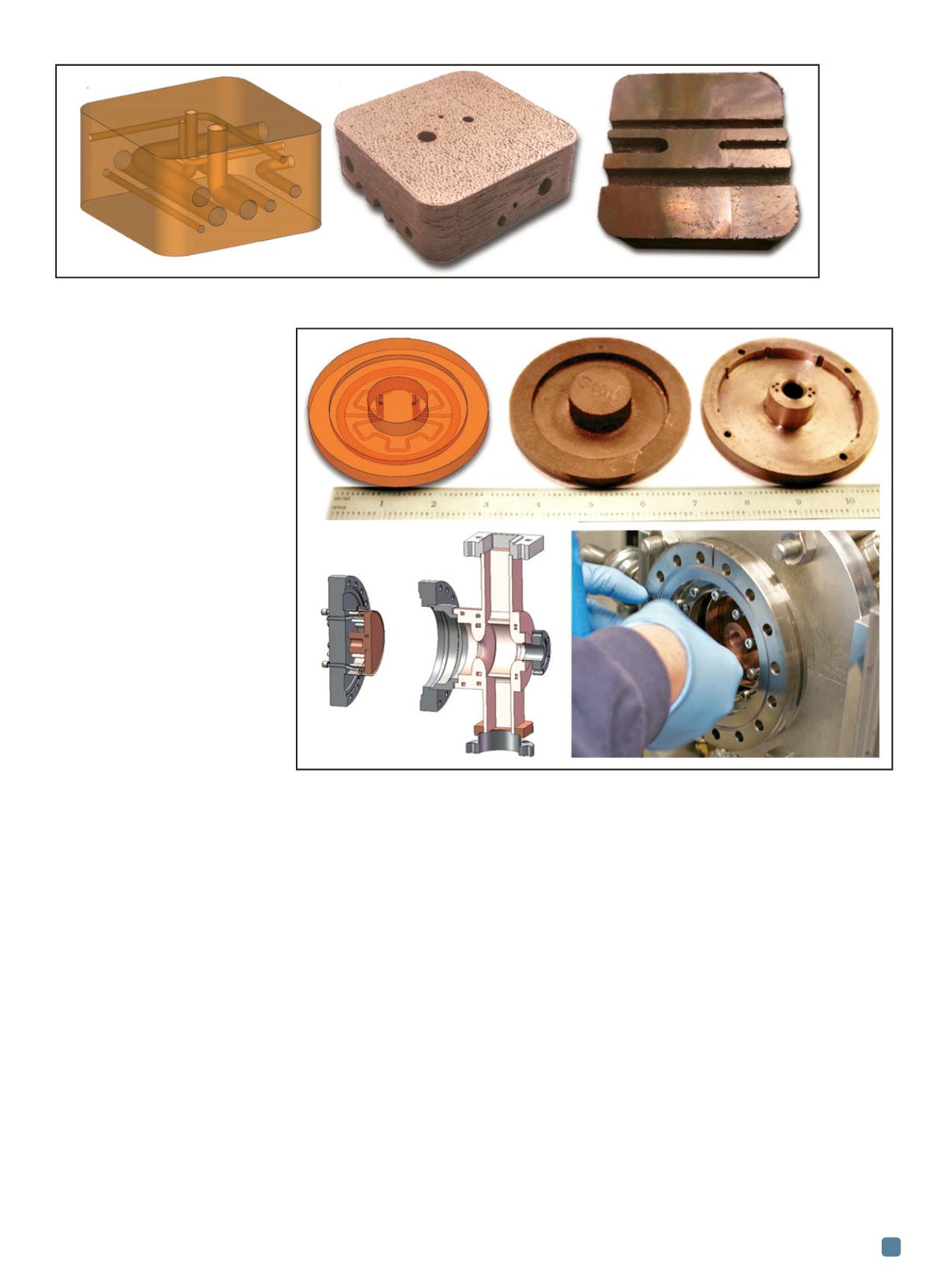
Cathode high power RF testing
In order to verify RF performance of the EBM copper,
a copper cathode suitable for testing in the UCLA Pegasus
1.6 cell photoinjector also was fabricated using the process
parameter sets developed during initial experiments. An
example is shown in Fig. 5. Figure 5 also shows the cathode
in the as-EBM condition, after final machining, and being
installed in the Pegasus photoinjector (Fig. 5e). No other
heat treatment was carried out on the EBM cathode prior
to final machining.
The EBM copper cathode performed as well as other
cathodes conventionally machined from wrought oxygen-
free (OFE) copper material during high power RF testing.
Stable operation with 70 MV/m peak electric fields on the
cathode was achieved after two hours of RF conditioning. A
photoelectron beam with energy of 3.3 MeV and charge of
60 pC was measured, along with a cathode quantum effi-
ciency of ~2x10
-5
. These numbers are consistent (given the
operating gradient) with conventional OFE copper cathodes
measured in the past at the Pegasus Laboratory.
Conclusions
Although the high thermal conductivity of copper
presents challenges for direct AM processes, fully dense
copper components with complex geometries were
demonstrated. Of particular interest is the ability to fabri-
cate internal cooling channels and mesh structures to op-
timize thermal management. In addition to EBM
processing parameters, oxidation of the copper powder
was found to hinder the ability to make completely suc-
Fig. 4
—
3D CAD model of the cooling channel test block shows internal cooling channel geometry (a); photographs of the
sectioned EBM-fabricated test blocks show cooling channels of 1.5, 4, and 7 mm in diameter (b and c).
Fig. 5
—
CAD rendering shows internal cooling channels of proposed EBM fabricated cathode offered
as a standard drop-in replacement by RadiaBeam (a); photograph of the cathode blank in the as-EBM
condition (b), and after final machining (c); CAD rendering of the RadiaBeam prototype freeform
cathode and freeform photoinjector (d); and installation in the UCLA Pegasus 1.6 cell Photoinjector (e).
(a) (b) (c)
(a) (b) (c)
(d) (e)