


 10 / 50

news
industry
briefs
Researchers at
University of
California Santa Barbara
created
a compound semiconductor of
nearly perfect quality with
embedded nanostructures
containing ordered lines of atoms
that can manipulate light energy in
the mid-infrared range. More
efficient solar cells, better
biological imaging, and the ability
to transmit massive amounts of
data at higher speeds are potential
applications. Erbium, which can
absorb light in the visible as well
as infrared wavelength, is key to
the technology. Erbium was paired
with antimony and the resulting
compound was embedded as
semimetallic nanostructures within
the semiconducting matrix of
gallium antimonide.
engineering.ucsb.edu.
An artist’s concept
of nanometer-size
metallic wires and
metallic particles
embedded in
semiconductors.
Courtesy of Peter
Allen.
Nanyang Technological
University (NTU),
Singapore,
launched a new $30 million 3D
printing facility to study medical
devices and tissue printing, among
other applications. The NTU
Additive Manufacturing Centre
(NAMC) also signed a $5 million
joint laboratory agreement with
SLM Solutions,
Germany, a 3D
printer manufacturer. Named
SLM
Solutions@NAMC,
the lab aims to
develop next-generation 3D
printers that can print very large
parts using new types of materials.
It will also develop platforms that
can print multiple materials in a
single build.
www.ntu.edu.sg.
3D-printed jewelry displayed at
the NTU Additive Manufacturing
Centre debut. Courtesy of NTU.
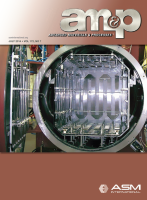
Newmethod enables industrial scale graphene production
Researchers at Massachusetts Institute
of Technology (MIT), Cambridge, and the
University of Michigan, Ann Arbor, dis-
covered a way to produce graphene in a
process that lends itself to scaling up, by
making graphene directly on materials
such as large sheets of glass. Currently,
most methods first grow the material on a
film of metal, such as nickel or copper, ex-
plains MIT mechanical engineering pro-
fessor A. John Hart. “To make it useful,
you have to get it off the metal and onto a
substrate, such as a silicon wafer or a poly-
mer sheet, or something larger like a sheet of glass,” he says. “But the process of transfer-
ring it has become much more frustrating than the process of growing the graphene itself,
and can damage and contaminate the material.”
The new work, Hart says, still uses a metal film as the template—but instead of mak-
ing graphene only on top of the metal film, the process makes it on both sides. The sub-
strate in this case is silicon dioxide, with a film of nickel on top. Using chemical vapor
deposition (CVD) to deposit a graphene layer on top of the nickel film yields graphene on
both sides. The nickel film can then be peeled away, leaving just the graphene on top of the
nonmetallic substrate. This eliminates the need for a separate process to attach the
graphene to the intended substrate
. For more information: A. John Hart, 617.324.7022,
ajhart@mit.edu,
mechanosynthesis.mit.edu.
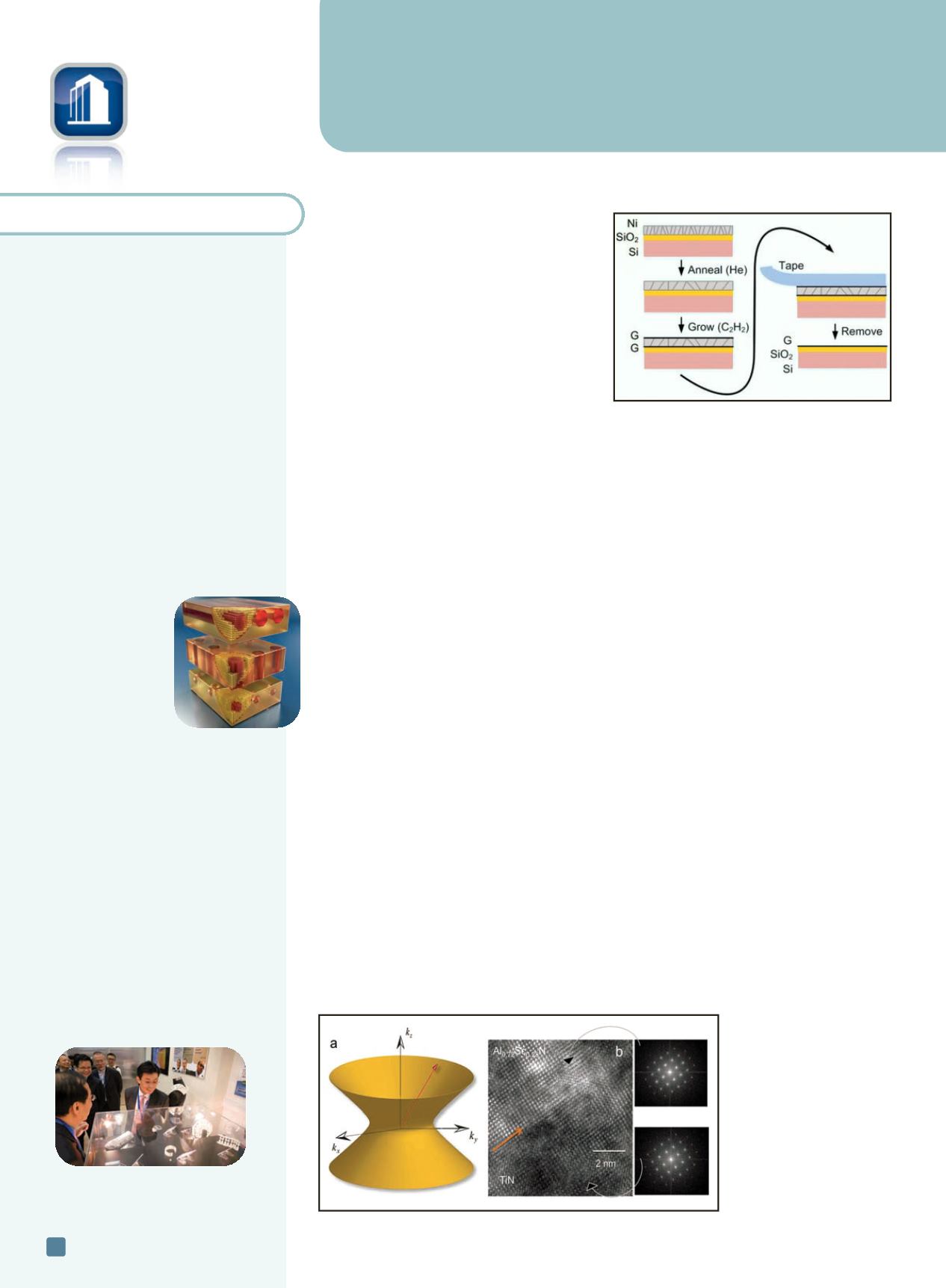
Hyperbolic metamaterials one step closer to reality
Researchers at Purdue University, West Lafayette, Ind., took another step toward practi-
cal applications for
hyperbolic metamaterials,
ultrathin crystalline films that could bring op-
tical advances including powerful microscopes, quantum computers, and high-performance
solar cells. New developments are similar to advances that ushered in silicon chip technol-
ogy, says Alexandra Boltasseva, associate professor of electrical and computer engineering.
Metamaterials have engineered surfaces that contain features, patterns, or elements,
such as tiny antennas or alternating layers of nitrides that enable unprecedented control of
light. Under development for about 15 years, metamaterials owe their unusual potential to
precision design on the nanometer scale. Optical metamaterials harness clouds of elec-
trons called surface plasmons to manipulate and control light. However, some of the plas-
monic components under development rely on using metals such as gold and silver, which
are incompatible with the complementary metal-oxide-semiconductor (CMOS) manufac-
turing process used to construct integrated circuits and do not transmit light efficiently.
Now, researchers created superlattice crystals from layers of titanium nitride and alu-
minum scandium nitride. The superlattices were created with epitaxy, and the layers were
grown inside a vacuum chamber using magnetron sputtering.
purdue.edu.
ADVANCED MATERIALS & PROCESSES •
JULY 2014
10
E
MERGING
T
ECHNOLOGY
Illustration of a new process for making
graphene directly on a nonmetal substrate.
Courtesy of the researchers.
A metamaterial’s hyperbolic
dispersion of light, left. At
center is a transmission
electron microscope image
showing the interface of
titanium nitride and
aluminum scandium nitride
in a superlattice. Two
images created using fast
Fourier transform to see
individual layers in the
material, right. Courtesy of
Purdue University.