



 27 / 58

edfas.org
27
ELECTRONIC DEVICE FAILURE ANALYSIS | VOLUME 19 NO. 2
interface. Often, APT laser power, evaporation rate, or
other parameters arealtered tohelpwithfieldevaporation
through delicate or problematic interfaces to avoid pre-
mature tip rupture. However, it is important tounderstand
the effects of altering such parameters on the integrity of
the collecteddata. For example, increasing the laser power
to assist field evaporation of a thin oxide layer may force
the overall evaporation field in the surrounding silicon
to stray from optimal. Likewise, decreasing the evapo-
ration rate when moving through a region of insulating
materials (e.g., gate oxide or spacer) to keep the tip from
fracturingmay significantly increase noise levels, making
low dopant profiles in nearby SiGe source/drain regions
more difficult to measure. These various trade-offs must
be considered, and remaining artifacts, noise, and so
on must be understood and properly interpreted if they
cannot yet be eliminated.
CONCLUSION
Atom probe tomography has a unique capability to
analyze even the most complex structures. Its combina-
tion of structural and chemical information for buried
nanostructures makes it a one-of-a-kind resource in a
number of fields and particularly for semiconductor
devices. Atom probe tomography helps provide a clearer
understanding of the shape and elemental composition
of complex device structures and light dopant profile
throughout these structures. Although many challenges
still remain for samplepreparation, improvedunderstand-
ing of APT data collection, and, most significantly, elimi-
nation of artifacts from the reconstructed 3-D data, APT
remains a powerful tool for failure analysis and research
and development of the next generation of advanced
semiconductor devices.
REFERENCES
1. A.J. Martin, W. Weng, Z. Zhu, R. Loesing, J. Shaffer, and A. Katnani:
“Cross-Sectional Atom Probe Tomography Sample Preparation for
Improved Analysis of Fins on SOI,”
Ultramicroscopy,
2016,
161
, pp.
105-09.
2. A.J. Martin, A.H. Hunter, T.W. Saucer, V. Sih, E.A. Marquis, and J.
Millunchick: “Atom Probe Tomography Analysis of Different Modes
of Sb Intermixing inGaSbQuantumDots andWells,”
Appl. Phys. Lett.,
2013,
103
, p. 122102.
3. A.K. Kambham, J. Mody, M. Gilbert, S. Koelling, and W. Vandervorst:
“Atom-Probe for FinFET Dopant Characterization,”
Ultramicroscopy,
2011, pp. 535-39.
4. D.R. Diercks, J. Tong, H. Zhu, R. Kee, G. Baure, J.C. Nino, R. O’Hayre,
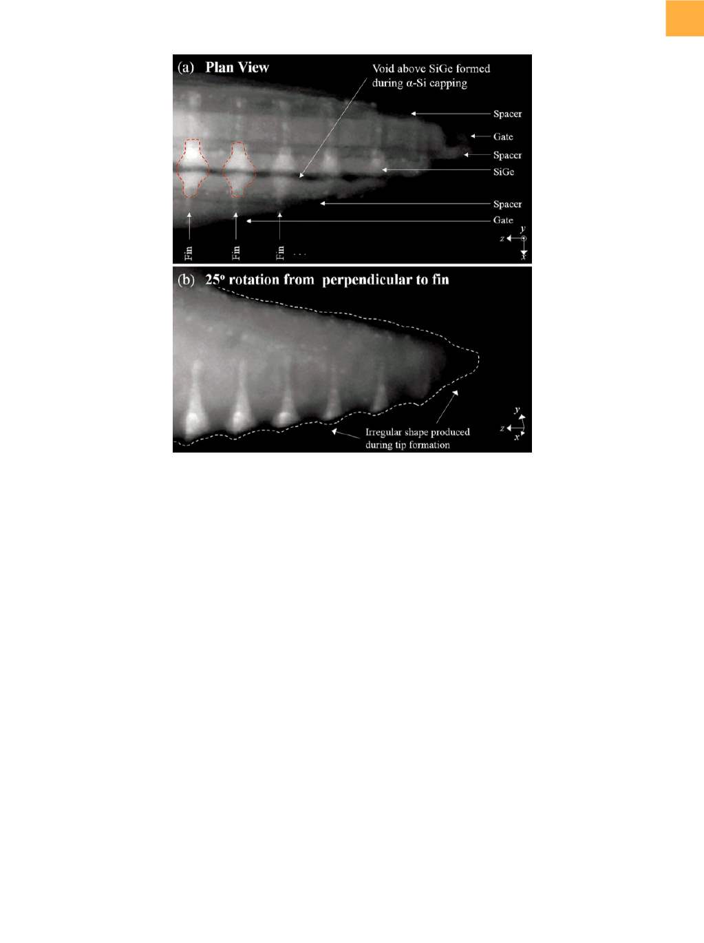
Fig. 7
STEM images of a different APT tip shaped from the same sample. (a) Plan-view perspective of the tip with various
features labeled. (b) Rotated view of the SiGe, highlighting the wavy shape of the outer surface of the tip. Scale bars
not shown for proprietary reasons
(continued on page 30)