


 32 / 58

edfas.org
ELECTRONIC DEVICE FAILURE ANALYSIS | VOLUME 19 NO. 2
32
characterization of nanopatterned metal and low-k
dielectrics.
[4]
Their results demonstrated the sensitivity
of the technique to isolate chemical modifications by
the interconnect fabrication process. This article dem-
onstrates the chemical characterization of the nanoscale
skin and polyester contaminants on a silicon wafer using
resonance-enhanced AFM-IR spectroscopy.
RESONANCE-ENHANCED AFM-IR
In the AFM-IR technique, the IR spectral intensity is
recorded in terms of mechanical force experienced by
an AFM cantilever due to photothermal expansion of the
absorbingmolecules. Adetailed account of the underlying
theory and correlation between optical, mechanical, and
thermal properties in AFM-IR are described elsewhere
[5]
and are beyond the scope of this report. It has been
demonstrated that the AFM-IR technique detects only
the heating and thermal expansion perturbations directly
underneath the AFM tip; spatial resolution is significantly
below the optical diffraction limit of the IRwavelength.
[5,6]
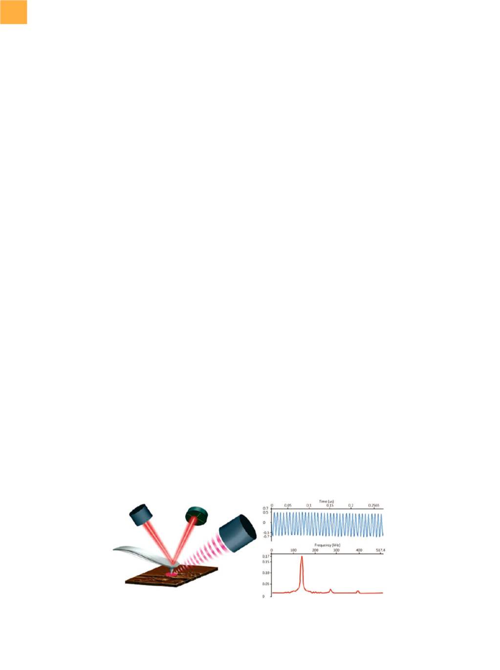
Resonance-enhanced AFM-IR was introduced to
enhance the sensitivity of the traditional AFM-IR for
thinner samples by using a high and tunable repetition-
rate IR source—quantum cascade lasers (QCLs).
[7,8]
This
pulse-rate tunability allows the user to synchronize the
laser pulses with a resonance frequency of the AFM can-
tilever. This synchronized pulsing gives rise to a high IR
sensitivity mode due to resonance enhancement of the
cantilever oscillation, typically providing a gain in sensitiv-
ity by a factor of 30 to 50 (Fig. 1).
The QCL source for the resonance-enhanced mode
has recently been upgraded to allow faster acquisition of
spectra over the full tuning range, allowing a reduction in
spectral acquisition time of a factor of 10 to 100. Earlier,
the data acquisition took place by stepping to eachwave-
number and measuring the oscillation amplitude of the
AFM cantilever to collect the AFM-IR spectrum. In the new
implementation, the QCL is swept over its range, and the
cantilever oscillation amplitude is measured simultane-
ouslywith thewavelengthchange. This enables significant
advancements in the data-acquisition protocol and vastly
impacts the measurement throughput by allowing faster
sample analysis or more data averaging. In addition, the
faster spectra can diminish the effects of thermal drift,
which improves the robustness and reproducibility of
the site-specific data, especially for dimensions
<
100 nm.
Combinedultrahigh sensitivity and fast spectral acqui-
sition in the resonance-enhancedmode has a tremendous
impact by allowing widespread use of nanoscale IR spec-
troscopy for spatially resolved chemical characterization
of nanoscale materials down to a thickness of 1 nm.
APPLICATIONS OF RESONANCE-
ENHANCED AFM-IR IN FAILURE
ANALYSIS
Contaminated silicon wafers were prepared in the
lab, using known materials typical of those found in the
semiconductor fab environment, and analyzed. For each
sample, high-resolution tapping-mode AFM images were
acquired to locate the contaminants, followed by the
AFM-IR measurements.
The tapping-mode AFM height image (Fig. 2a) illus-
trates the thickness variation (20 to 100 nm) of the con-
taminant residue (human skin tissue) on one of the test
siliconwafers. After locating the desired site from the AFM
image, the QCL pulse rate is tuned to one of the cantilever
oscillation modes (~170 kHz, 2nd mode), and the laser is
swept in the fast-acquisitionmode to acquire resonance-
enhanced AFM-IR spectra (Fig. 2b). The measurements
were performed at sites with varied thicknesses (20 to
100 nm), as indicated in Fig. 2. Observed IR intensity
Fig. 1
(a) Resonance-enhanced AFM-IR operation: rapid thermal expansion experienced by AFM cantilever subsequent to IR
absorption. (b) Cantilever oscillations due to IR absorption and (c) fast Fourier transformof the oscillation signal. Laser
pulse rate is tuned to cantilever oscillation mode for resonance enhancement.