


 30 / 58

edfas.org
ELECTRONIC DEVICE FAILURE ANALYSIS | VOLUME 19 NO. 2
30
ADVANTAGES AND CHALLENGES OF 3-D ATOM PROBE TOMOGRAPHY
(continued from page 27)
andB.P.Gorman:“Three-DimensionalQuantificationofComposition
and Electrostatic Potential at Individual Grain Boundaries in Doped
Ceria,”
J. Mater. Chem. A,
2016,
4
, pp. 5167-75.
5. S.S. Rout, P.R. Heck, D. Isheim, T. Stephan, A.M. Davis, and D.N.
Seidman: “Correlative TEM and Atom-Probe Tomography of a
Kamacite-Taenite Interface in the Bristol IronMeteorite,”
46th Lunar
Planetary Sci. Conf.,
2015, p. 2938.
6. T.F. Kelly, O. Nishikawa, J.A. Panitz, and T.J. Prosa: “Prospects for
Nanobiology with Atom-Probe Tomography,”
MRS Bull.,
2009,
34
,
pp. 744-49.
7. E.A. Marquis, M. Bachhav, Y. Chen, Y. Dong, L.M. Gordon, and A.
McFarland: “On the Current Role of Atom Probe Tomography in
Materials Characterization and Materials Science,”
Curr. Opin. Solid
State Mater. Sci.,
2013,
17
, pp. 217-23.
8. B. Gault, M.P. Moody, F. de Geuser, A. la Fontaine, L.T. Stephenson,
D. Haley, and S.P. Ringer: “Spatial Resolution in Atom Probe
Tomography,”
Microsc. Microanal.,
2010,
16
, pp. 99-110.
9. B. Gault, M.P. Moody, F. de Geuser, D. Haley, L.T. Stephenson, and S.P.
Ringer: “Origin of the Spatial Resolution in AtomProbeMicroscopy,”
Appl. Phys. Lett.,
2009,
95
, p. 034103.
10. A.J. Martin, J. Hwang, E.A. Marquis, E. Smakman, T.W. Saucer, G.V.
Rodriguez, A.H. Hunter, V. Sih, P.M. Koenraad, J.D. Philips, and J.M.
Millunchick: “The Disintegration of GaSb/GaAs Nanostructures upon
Capping,”
Appl. Phys. Lett.,
2013,
102
, p. 113103.
11. E.A. Jagle, P.P Choi, and D. Raabe: “The Maximum Separation
Cluster Analysis Algorithm for Atom Probe Tomography: Parameter
Determination and Accuracy,”
Microsc. Microanal.,
2014,
20
, pp.
1662-71.
12. K. Thompson, D. Lawrence, D.J. Larson, J.D. Olson, T.F. Kelly, and B.
Gorman: “In Situ Site-Specific SpecimenPreparation for AtomProbe
Tomography,”
Ultramicroscopy,
2007,
107
, pp. 131-39.
13. D.J. Larson, T.J. Prosa, R.M. Ulfig, B.P. Geiser, and T.F. Kelly:
Local
Electrode Atom Probe Tomography,
Springer, New York, 2013.
14. B.P. Geiser, D.J. Larson, E. Oltman, S. Gerstl, D. Reinhard, T.F. Kelly,
and T.J. Prosa: “Wide-Field-of-View Atom Probe Reconstruction,”
Microsc. Microanal.,
2009,
15
(Suppl. 2), pp. 292-93.
15. B. Gault, D. Haley, F. de Geuser, M.P. Moody, E.A. Marquis, D.J. Larson,
and B.P. Geiser: “Advances in the Reconstruction of Atom Probe
Tomography Data,”
Ultramicroscopy,
2011,
111
, pp. 448-57.
16. D.J. Larson, B.P. Geiser, T.J. Prosa, and T.F. Kelly: “On the Use of
Simulated Field-Evaporated Specimen Apex Shapes in Atom Probe
Tomography Data Reconstruction,”
Microsc. Microanal.,
2012,
18
,
pp. 953-63.
17. J.H. Lee, B.H. Lee, Y.T. Kim, J.J. Kim, S.Y. Lee, K.P. Lee, and C.G. Park:
“Study of Vertical Si/SiO
2
Interface Using Laser-Assisted AtomProbe
Tomography and Transmission Electron Microscopy,”
Micron,
2014,
58
, pp. 32-37.
18. F. Vurpillot and C. Oberdorfer: “Modeling Atom Probe Tomography:
A Review,”
Ultramicroscopy,
2015,
159
, pp. 202-16.
19. F. Vurpillot, B. Gault, B.P. Geiser, and D.J. Larson: “Reconstructing
Atom Probe Data: A Review,”
Ultramicroscopy,
2013,
132
, pp. 19-30.
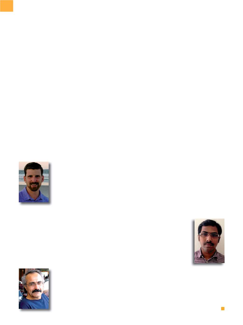
ABOUT THE AUTHORS
Andrew J. Martin
is part of the Advanced Technology Development organization at
GLOBALFOUNDRIES, where he works exclusively on atom probe tomography research and develop-
ment for advanced characterization of the next generation of FinFET technology. Dr. Martin received
his B.S. degree from Purdue University and his Ph.D. in materials science and engineering from the
University of Michigan, where he studied growth and characterization of quantum dots for solar cell
applications andwas first introduced to theworld of APT. He co-authoredmore than 15 papers during
his tenure. Dr. Martin enjoys doing hands-on work with APT sample preparation and designing novel
instrumentation and techniques for advancing the scope of APT analysis and its impact on device
research and development at GLOBALFOUNDRIES. He is also an adjunct assistant professor at Columbia University, where
he has taught in the Materials Science and Engineering Department since 2014.
Ajay Kumar Kambham
received his B.Sc. and M.Sc. (physics) degrees from Sri Venkateswara
University, Tirupati, India, in 2001 and 2005, respectively. He obtained a second Master’s (M.Tech)
degree in materials science from Indian Institute of Technology Delhi, New Delhi, India, in 2008. In
2013 he received his Ph.D. in physics (“Atomic Scale Characterization of 3-D Structures with Atom
Probe Tomography”) from IMEC and the University of Leuven, Belgium. Soon after completing his
Ph.D., Dr. Kambham joined GLOBALFOUNDRIES, Malta, N.Y. He is currently a principal engineer in the
Center for Complex Analysis, supporting fab activities on current subnanotechnology nodes from
planar to FinFET structures by performing atom probe analysis.
AhmadD. Katnani
received his Ph.D. in physics fromtheUniversity of Wisconsin-Madison in 1983.
He has held various engineering and management positions at IBM microelectronics and supply
chain divisions. Currently, he manages a failure and materials analysis team at GLOBALFOUNDRIES,
East Fishkill, N.Y.