


 26 / 58

edfas.org
ELECTRONIC DEVICE FAILURE ANALYSIS | VOLUME 19 NO. 2
26
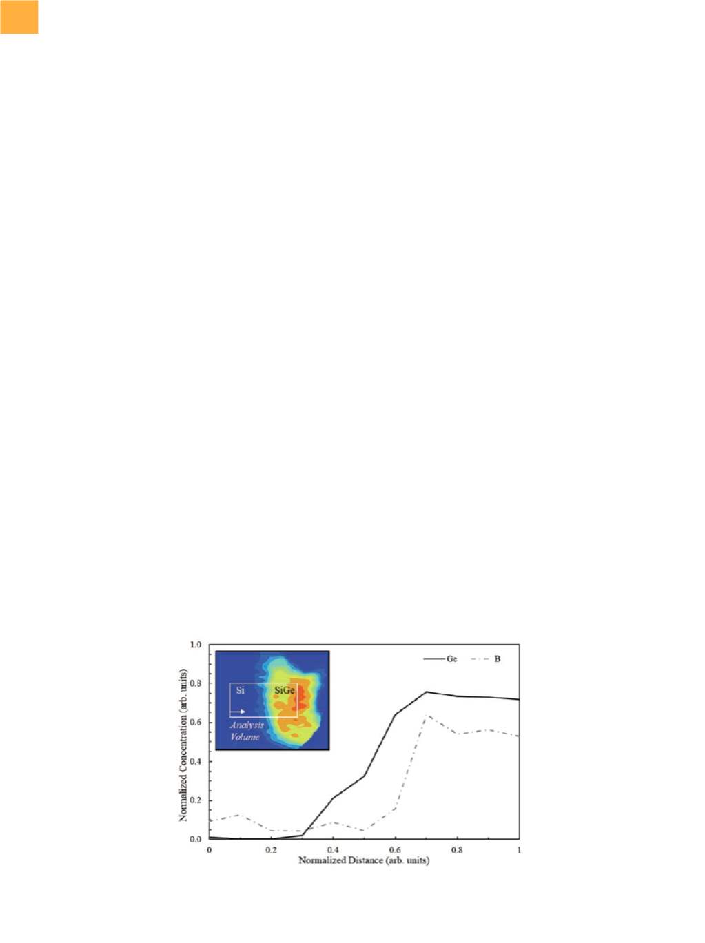
plan viewperspective (Fig. 5b) of the SiGe. Figure 6 shows
a plot of the germaniumand boron concentrations across
the transition from the silicon fin to the SiGe source/drain
region. The dashed white line in Fig. 5(b) highlights the
faceted profile in the
x
-
z
plane. A distortion in the APT
reconstruction causes the SiGe profile in the bottom right
of Fig. 5(b) to skew toward the top of the tip (negative
z
-direction). Scanning transmission electron microscopy
(STEM) images in Fig. 7(a), which were taken on another
APT tip from the same sample, confirm this “plus” sign,
faceted shape. The originof this distortion to the SiGe is an
undulating shape along the outer surface of the tip from
one fin to the next along the
z
-axis. This wavy pattern,
highlighted in Fig. 7(b), was formed as a result of differ-
ing FIB milling rates of the SiGe and neighboring oxide
during tip shaping. A combination of more complex field
evaporation due to the wavy shape and the assumption
of a smooth outer surface by the reconstruction algorithm
leads to some distortion along this surface. Minimizing
distortions such as this and accurately understanding
their source are just some of the many challenges facing
the development of APT for semiconductor devices.
CHALLENGES IN APT
As APT matures into a staple characterization tech-
nique in a variety of fields, more and more challenges
are continually met. Atom probe tomography in all fields
of study will always face the challenge of improving our
understanding of the field-evaporationprocess for various
materials, particularly at interfaces, as well as reconstruc-
tion accuracy. This is particularly the case for samples
containing layers, thin films, or isolated regions with very
differing evaporation fields from the bulk of the sample.
Much work has been done in both experimentation and
simulation to understand the field-evaporation process
in these situations and how to improve the reconstruc-
tion.
[16-19]
Semiconductor devices perhaps embody this
challenge more than most other fields because, by
nature, they contain a complex arrangement of metals,
semiconductors, and insulators in close proximity. Even
oxides as thin as a couple nanometers can create artifacts
in neighboring semiconductor materials.
[1]
For semicon-
ductor devices, the primary challenges facing APT can be
grouped into three categories:
• Sample preparation
• Fieldevaporation throughdissimilarmaterial interfaces
• Elimination and proper interpretation of reconstruc-
tion artifacts
Isolating small or specific features on the nanoscale in
the FIB is never easy. This is certainly true for semiconduc-
tor devices. This is further complicated by the fact that
APT sample preparation requires isolating features in a
conical tip rather than a planar lamella, as is the case for
TEM. Differences in milling rates between different mate-
rials within semiconductor devices (e.g., SiGe compared
to gate oxide) make it difficult to achieve the ideal tip
shape necessary to satisfy the assumptions made by the
reconstruction algorithm. Tip shaping is often as much of
an art as a developed skill, and creativity in approaching
different structures inuniqueways canoften reapbenefits
through thorough planning and meticulous preparation.
Field evaporation through interfaces of dissimilar
materials requires aproper understandingof thematerials
involved and their order/orientation in order to optimize
the APT operating conditions while passing through the
Fig. 6
Germanium and boron profiles plotted frommeasurements across the silicon-to-SiGe transition of the fin, as indicated
in the inset