


 8 / 58

edfas.org
ELECTRONIC DEVICE FAILURE ANALYSIS | VOLUME 19 NO. 1
8
The difference from the BGA in Fig. 8 is that the molten
solder ball did not wet the surface of the PCB land. The
faulty solder print could also be identified next to the
defective BGA on a bare printed pattern without an
assembled BGA (Fig. 11). Once again, the root cause of
the failure was a dried-out, clogged stencil while printing
the solder paste.
SUMMARY
Based on a number of case studies, it was shown that
failuremay originate at a number of steps in themanufac-
turing process, for example, fromthe solder paste printing
process or from the soldering process itself. The stencil
printing of the solder paste is often a critical process, but
more often, the root cause is faulty PCBs.
Cross sections of solderedBGAs are common for failure
analysis. One newapproach is presented as an additional
method in the course of finding the root cause of failures.
Grinding away the corpus of the BGA until the soldered
balls are still left on the PCB can provide insight into the
failure mechanism.
In the case of perfect solder connections, grinding the
PCB from the backside is another approach, whichwill be
discussed in Part II of this article in the May issue of
EDFA
.
ABOUT THE AUTHOR
Gert Vogel
studied physics in
Stuttgart. He has been with Siemens
for more than 30 years. Dr. Vogel
was a semiconductor technologist
in Siemens’ DRAM production in
Munich and Regensburg for seven
years. He then moved to Siemens
Amberg where, among other topics, he is a specialist
in failure analysis of electronic components on printed
circuit board assemblies. He led a tutorial, “Avoiding
Flex Cracks in Ceramic Capacitors,” at ESREF 2015.
This was followed by a tutorial, “Creeping Corrosion
of Copper on Printed Circuit Board Assemblies,” at
ESREF 2016.
FAILURE ANALYSIS ON SOLDERED BALL GRID ARRAYS: PART I
(continued from page 6)
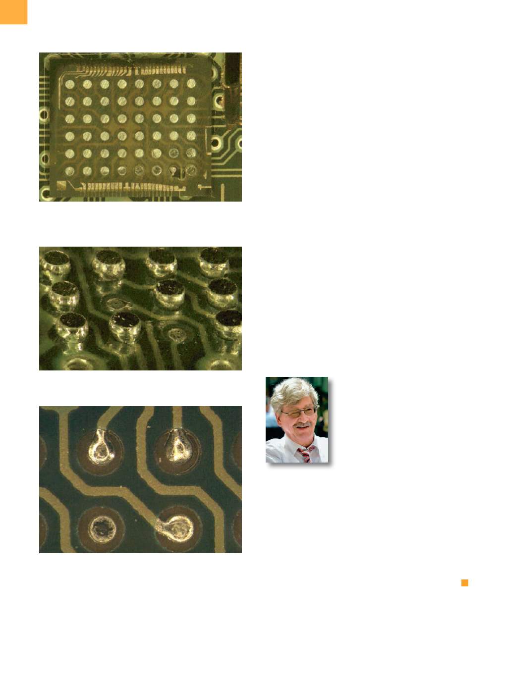
Fig. 9
After grindingdown theBGAandbeforeblowingaway
the residue of the solder resist fromthe bottomof the
BGA, it was discovered that one ball had dropped off.
Fig. 10
After blowing away the residue of the solder resist,
two missing balls can be seen.
Fig. 11
The faulty solder print can also be seen on a printed
patternwith the same geometry next to the defective
BGA.