


 10 / 58

edfas.org
ELECTRONIC DEVICE FAILURE ANALYSIS | VOLUME 19 NO. 1
10
TRAPS AND CHARGES
David Burgess, Accelerated Analysis
davidburgess@AcceleratedAnalysis.comI
mportant oxide characteristics are skipped over briefly
in basic descriptions of MOS operation. Oxide is not
even mentioned in descriptions of bipolar devices. In
fact, oxide and alternate insulators are critical to semi-
conductors. Identifying, avoiding, or eliminating inherent
problems was, and still is, a major focus for process
development.
At the time of the first lunar landing, mobile charges
in oxide were an important factor that limited reliability.
Today, modern processes and device design have largely
eliminated mobile charge failures. However, the mobile
charge failuremechanismremains andcould reappear any
time our defenses lapse. Mobile charge is designated
Q
m
.
Oxide traps, however, aremore important thanever.
Q
f
,
Q
it
, and
Q
ot
are designations for three types of oxide traps.
MOBILE IONS
Sodium and potassium ions have a positive charge
and move readily in silicon dioxide under influence of
an electric field. The electric charge of mobile ions has
maximumeffect when locatednear the underlying silicon.
Capacitance-voltage (CV) plotting is used during fabri-
cation to detect andmeasure the existence ofmobile ions.
CV plotting is also a goodway to understand the behavior
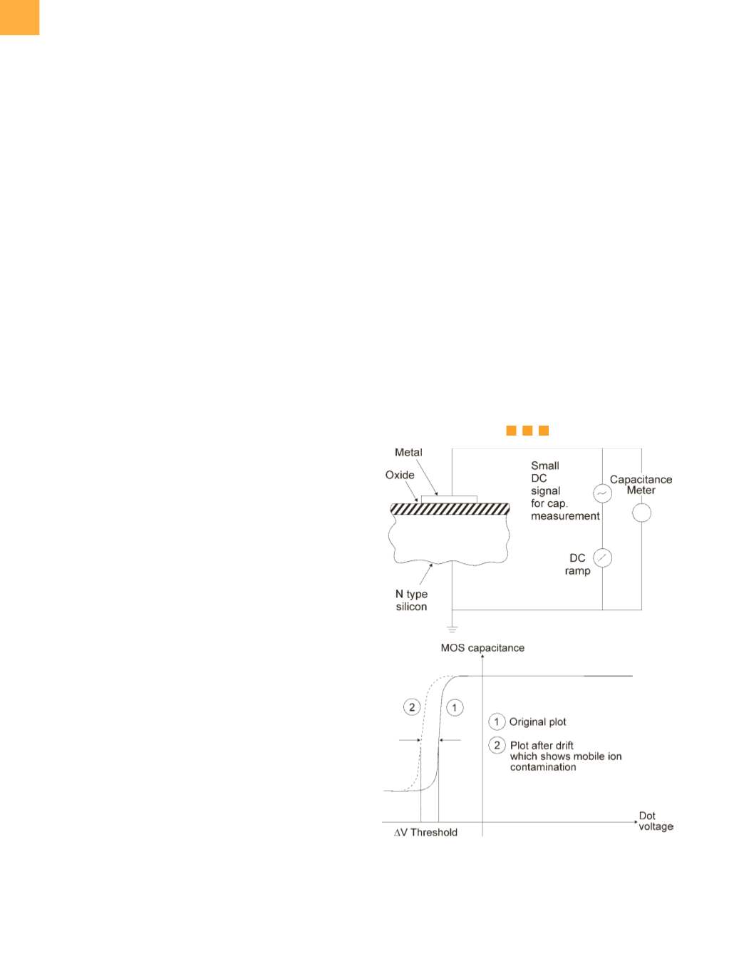
of mobile ions in oxide. A simple capacitor is shown in
Fig. 1(a), while typical CV plots are shown in Fig. 1(b).
The plots show capacitance corresponding to different
direct-current voltage applied to the metal dot. At suf-
ficiently negative applied voltage, electrons are repelled
from the surface of the silicon, causing a
P
-type inversion
layer. Measured capacitance is low because the effective
thickness of the capacitor is the oxide thickness plus
the inversion layer thickness. At higher applied voltage,
the inversion layer disappears. The effective insulator
thickness is equal to the oxide thickness alone, and the
capacitance increases correspondingly.
Sodium ions havemobility in oxide even at room tem-
perature. In the absence of an applied field, ions in the
oxide will spread evenly through the oxide. Mobile ions
EDFAAO (2017) 1:10-13
1537-0755/$19.00 ©ASM International
®
“TODAY, MODERN PROCESSES AND
DEVICE DESIGN HAVE LARGELY
ELIMINATED MOBILE CHARGE FAILURES.
HOWEVER, THE MOBILE CHARGE
FAILURE MECHANISM REMAINS AND
COULD REAPPEAR ANY TIME OUR
DEFENSES LAPSE.”
(a)
(b)
Fig. 1
(a) Simple capacitor. (b) Two CV plots of metal oxide
siliconstructure.Plot1takenonsampleas-fabricated;
mobile charge is distributed throughout oxide. Plot
2 taken after high-temperature drift; mobile charge
is focused at oxide/silicon interface.