


 5 / 58

edfas.org
5
ELECTRONIC DEVICE FAILURE ANALYSIS | VOLUME 19 NO. 1
cause can only be revealed by thoroughly controlling all
of the parameters of the soldering process. Another clue
is the optical appearance of the solder balls after a second
reflow process, which is manifested by a creased skin of
tin oxide (Fig. 2).
With several special preparation techniques, many dif-
ferent sources of voiding can be clarified. The goal of the
analysis is always to clarify the root cause of the failure so
that it can be eliminated in the future. If the root cause has
been clearly identified, then an additional benefit is that
it may be possible to make a claim against the supplier.
ELECTRICAL FAILURES WITH EYE-
CATCHING X-RAY OBSERVATIONS
Even if electrical shorts are easily detectedby perform-
ing an x-ray analysis, the determination of the root cause
can still be very complicated. The following example
shows very clearly the short circuit between BGA balls
and adjacent through-holes in the x-ray image (Fig. 3)
as well as in the cross section (Fig. 4); however the root
cause must be searched for in the PCB. A bad immersion
tin rework underetched the solder resist aroundopenings.
It became brittle and flaked off, exposing bare copper that
facilitated the flowof liquid solder across the clearance to
the adjacent contacts (Fig. 5).
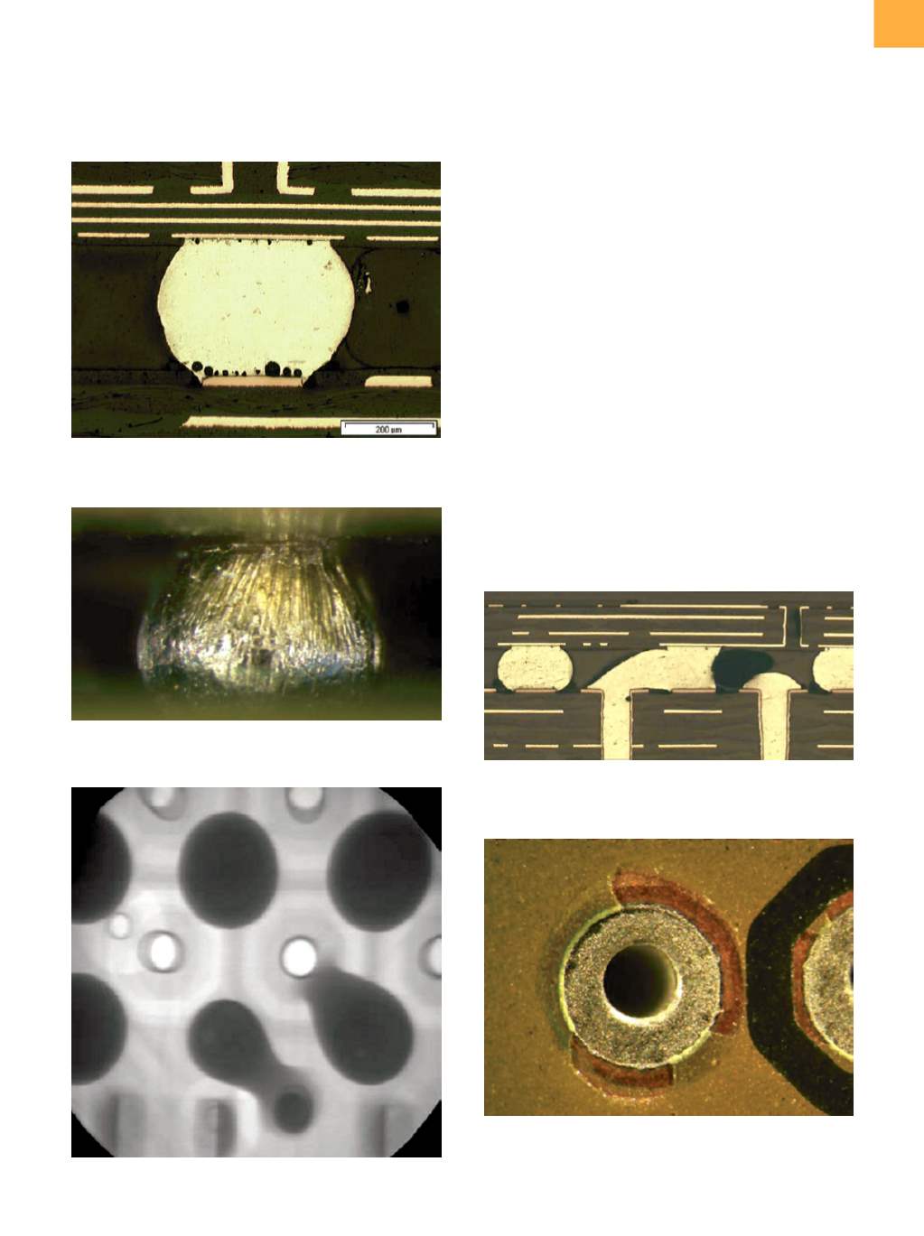
Fig. 1
Cross section through a BGA ball with so-called
“champagne voids”
Fig. 2
BGA balls with champagne voids manifest a creased
skin after a second reflow.
Fig. 3
X-ray image of solder faults at BGA balls
Fig. 4
Cross section of the solder faults from Fig. 3. Short
circuits causedbyflowing solder as a result ofmissing
solder resist
Fig. 5
Microscopic inspection of the surface of the PCB
reveals faulty solder resist. Underetched films broke
off, caused by a bad immersion tin rework.