


 11 / 58

edfas.org
1 1
ELECTRONIC DEVICE FAILURE ANALYSIS | VOLUME 19 NO. 1
diffuse away from regions of high concentration. The like
charge ofmobile ions causes themto repel eachother. The
original plot in Fig. 1(b) was taken while mobile charges
were evenly distributed. The step increase in capacitance
identifies the threshold voltage required to produce the
inversion layer.
Plot 2 in Fig. 1(b) was taken after a positive-voltage
high-temperature step to drift any positive ions down
to the silicon surface. Only a few seconds at 300 °C are
required to accumulate near the surface of the silicon.
After drifting ions toward the silicon, the capacitor was
allowed to cool under bias. Plot 2 was taken while ions
were focused near the silicon surface, where their effect is
at maximum. A greater negative voltage must be applied
to overcome the positive mobile ion and cause inversion.
The threshold voltage has shifted.
The difference in threshold voltage is a measure of
mobile ions present. The randomly uniform distribution
of mobile ions can be restored by baking without bias at
300 °C for a few seconds or at 125 °C for 24 h.
MOBILE IONS IN
PNP
TRANSISTORS
Failures of very early
PNP
devices illustrate more
characteristics of mobile ions. Actions to avoid
PNP
fail-
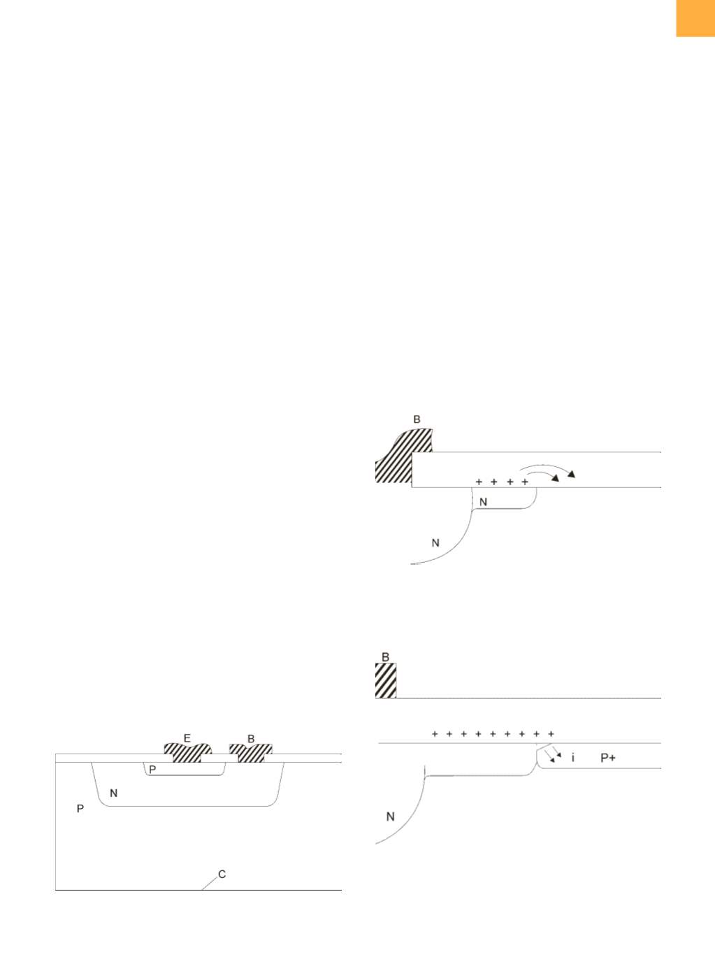
ures verify our conclusions. Figure 2 is a cross section of
a 1970 transistor. In normal operation, the base is biased
at a voltage higher than the collector voltage. An electric
“fringe” field exists in the oxide above the base/collection
junction. Mobile ions in the vicinity move away from the
base toward the collector. In time, mobile ions concen-
trated at the silicon surface attract electrons and invert
the silicon surface. As a result, the base spreads out into
the previous collector area. The electric fringe fieldmoves
to the new junction and expands the inverse further.
Figure 3 shows the expandedbase. At this point, transistor
parameters do not change drastically. The new junction
adds a small amount of leakage current. Breakdown of
the new diode is usually higher than the original collec-
tor/base diode.
However, the inversion ultimately reaches the edge of
the silicon chip. Current flows directly from base to col-
lector through the inversion layer. The edge of the chip
provides a leakage path. The collector/base I/V charac-
teristic becomes a classic channel current.
A first attempt to avoid channel current was to add
a
P
+
“channel stop.” The idea was that the
P
ring would
be too highly doped to allow inversion. In fact, the edge
of the heavily doped
P
ring did invert. The depth of the
inversion was so shallow that electrons simply tunneled
through
[1]
(Fig. 4).
A successful remedywas to add ametal ring contacted
to the
P
ring. The metal and the silicon directly below are
at the same voltage. No electric field exists under the ring.
Lacking an electric field, the inversion cannot expand
under the metal (Fig. 5).
Fig. 2
Schematic cross section of basic
PNP
transistor
Fig. 3
Schematic cross section showing inversion induced
by mobile charge. Electric fringe field is associated
with the new junction edge.
Fig. 4
Schematic cross section showing tunnel current at
edge of ineffective
P
+
channel stop. The inversion
cannot proceed, but the leakage path is established.