


 6 / 58

edfas.org
ELECTRONIC DEVICE FAILURE ANALYSIS | VOLUME 19 NO. 1
6
PLANE PARALLEL POLISHING OF A BGA
TO OBTAIN JUST THE BALLS
If x-ray analysis and optical microscopy provide no
clues for why there is an open circuit between BGA balls
and the PCB, if different sizes of BGA balls are visible, or if
the BGA is sensitive to coolant spray (intermittent open),
then a more drastic approach may be advisable than
just a simple cross section through some of the solder
joints. If you want to analyze those joints, and something
prevents you from looking at them, then remove anything
that hinders you. Thismeans grinding and polishing away
the complete BGA, leaving only the balls (Fig. 6). After this
procedure, one can use a needle to verify whether the
solder joint ismechanically stable, and every ball can also
be inspected from every direction (Fig. 7). A cross section
can still be obtained through the PCB and the solder ball.
The grinding down and polishing of a BGAwith an area
of several square centimeters is not as complicated as it
may appear. It can be done by hand with an accuracy of
better than 10 µm, because a multitude of copper layers
in the BGA help the operator keep in parallel. As soon as
the first shiny, silvery small dots appear, one must be
very careful, because the last layer of the BGA has been
reached. The solder resist around the solder balls cannot
be polished away but must be blown off.
The solder balls of the BGA in Fig. 8 manifested dif-
ferent diameters when performing the x-ray inspection.
Preparation by grinding down the BGA reveals the root
cause: There are no flux residues around the balls having
a smaller diameter. This means there is only the solder
material of the BGA ball but no printed solder paste,
probably because the stencil was dried out and clogged.
TYPICAL ERROR PATTERN: COLD JOINT
An electrical open circuit was found in the next case.
An x-ray examination showed no abnormalities. The BGA
was polished down, and just before blowing off the solder
resist, a lost solder ball was identified (Fig. 9). Detailed
inspection showed that two balls dropped away. The
solder pads showed no flux and no solder paste (Fig. 10).
(continued on page 8)
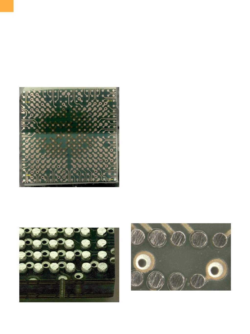
Fig. 6
Removal of the body of the solderedBGA by polishing
it down fromthe top of the BGA. Preparationby plane
parallel grinding of the BGA shows some warpage in
the soldered BGA. On the left, the PCB of the BGA has
already been polished down to the silvery, shining
top of the first balls.
Fig. 7
After exposing all of the balls and blowing away the
rest of the solder resist, the balls can be inspected
fromall sides. No soldering problemswere identified.
Fig. 8
In this case, the root cause for varying sizes of the
solder balls can easily be seen. Around some balls
there are no residues of flux. These balls also have a
smaller diameter, which means that no solder paste
was printed at these locations.