


 41 / 58

edfas.org
41
ELECTRONIC DEVICE FAILURE ANALYSIS | VOLUME 19 NO. 1
PRODUCT NEWS
Larry Wagner, LWSN Consulting Inc.
lwagner10@verizon.netPRESS RELEASE SUBMISSIONS:
MAGAZINES@ASMINTERNATIONAL.ORGFEI OFFERS EFA WORKFLOW
SOLUTIONS
Semiconductormanufacturers can turn to newelectri-
cal failure analysis (EFA) solutions for the tools required
to identify and analyze faults in their products. The new
nProber III fault localization and transistor character-
ization tool developed by FEI (Hillsboro, Ore.) provides
process development and failure analysis down to the 7
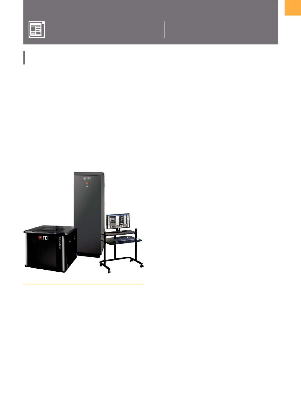
nmtechnology node. The newMeridian 7 optical fault iso-
lation tool, also developed by FEI, is designed to provide
the resolution needed for nondestructive localization of
electrical faults at sub-10-nm nodes.
extracting thin sectional samples for physical failureanaly-
sis in the TEM. In some critical applications, nanoprobing
canpotentially increase TEMsuccess rates. Designed tobe
an effective and easy-to-use tool, the nProber III doubles
the resolution and probe stability over its predecessor.
The new Meridian 7 provides visible laser voltage
imaging and probing as well as dynamic laser stimulation
on sub-10-nmdevices. By avoiding a requirement for ultra-
thin substrates, it preserves the integrity and functionality
of the device under test to provide a reliable and practical
production solution. It offers a 25% optical resolution
enhancement over the previous-generation system and
has a smaller spot size for better fault localization. In addi-
tion, thenewMeridian7offersmore certainty innavigation
and computer-aided design overlay, less cross-talk, and
higher waveform signal-to-noise over its predecessor.
For more information: web: bit.ly/2fLQZvH.
3-D NANOPRINTING IMPROVES AFM
PERFORMANCE
Tiny sensors made through nanoscale 3-D printing
may be the basis for the next generation of atomic force
microscopes (AFMs). These nanosensors can enhance the
microscopes’ sensitivity and detection speed by minia-
turizing their detection component up to 100 times. The
sensors were used in a real-world application for the first
time at École Polytechnique Fédérale de Lausanne (EPFL)
in Switzerland, and the results were published in
Nature
Communications.
The sensor ismade up of highly conduc-
tive platinum nanoparticles surrounded by an insulating
carbon matrix.
Atomic forcemicroscopy is basedonpowerful technol-
ogy that works a little like a miniature turntable. A tiny
cantilever with a nanometric tip passes over a sample
and traces its relief, atom by atom. The tip’s infinitesimal
up-and-down movements are picked up by a sensor so
that the sample’s topography can be determined. One
way to improve AFMs is to miniaturize the cantilever,
because this will reduce inertia, increase sensitivity, and
speed up detection. Researchers at EPFL’s Laboratory for
Bio- and Nano-Instrumentation achieved this by equip-
ping the cantilever with a 5-nm-thick sensor made with a
nanoscale 3-Dprinting technique. “Using ourmethod, the
FEI’s Meridian 7 optical fault isolation tool
“Automation is a high priority in our roadmap,” said
Cecelia Campochiaro, Vice President of EFA Solutions at
Thermo Fisher Scientific. “The nProber III system begins
ourmove toward automating the nanoprobing technique
by incorporating intelligent-guided operations designed
to improve time-to-results and reduce the skill required
to run the tool.”
These new solutions are part of a complete EFA
workflow that includes fault isolation, electrical probing,
delayering, sample preparation and imaging, and, when
needed, atomic-level imaging in a transmission electron
microscope (TEM). The nProber III allows FA engineers to
find and characterize individual devices preparatory to