


 42 / 58

edfas.org
ELECTRONIC DEVICE FAILURE ANALYSIS | VOLUME 19 NO. 1
42
cantilever can be 100 times smaller,” says Georg Fantner,
the lab’s director.
The nanometric tip’s up-and-downmovements can be
measured through the deformation of the sensor placed
at the fixed end of the cantilever. However, because the
researchers were dealing with minute movements—
smaller than an atom—they had to pull a trick out of their
hat. TogetherwithMichael Huth’s labat GoetheUniversität
at Frankfurt amMain, Germany, they developed a sensor
made up of highly conductive platinum nanoparticles
surrounded by an insulating carbonmatrix. Under normal
conditions, the carbon isolates the electrons. However,
at the nanoscale, a quantum effect comes into play:
Some electrons jump through the insulating material
and travel from one nanoparticle to the next. “It’s sort of
like if people walking on a path came up against a wall,
and only the courageous few managed to climb over it,”
said Fantner. When the shape of the sensor changes, the
nanoparticlesmove farther away fromeach other, and the
electrons jump between them less frequently. Changes in
the current thus reveal the deformation of the sensor and
the composition of the sample.
The researchers’ real feat was in finding a way to
produce these sensors in nanoscale dimensions while
carefully controlling their structure and, by extension,
their properties. “In a vacuum, we distribute a precursor
gas containing platinum and carbon atoms over a sub-
strate. Then we apply an electron beam. The platinum
atoms gather and form nanoparticles, and the carbon
atoms naturally form a matrix around them,” said Maja
Dukic, the article’s lead author. “By repeating this process,
we can build sensors with any thickness and shape we
want. We have proven that we could build these sensors
and that they work on existing infrastructures. Our tech-
nique can now be used for broader applications, ranging
from biosensors and antilock braking sensors for cars to
touch sensors on flexible membranes in prosthetics and
artificial skin.”
For more information: web: nature.com/articles/
ncomms12487.
ECONO BOARD PROBES ENHANCE
MEASUREMENTS
Econo Board probes are the first group released
from Oxford Instruments Asylum Research’s new line
of SurfRider probes. “Econo Board probes can be used
by all atomic force microscope users doing routine mea-
surements,” said Teimour Maleki, Director of MEMS and
Business Technology at AsylumResearch (Santa Barbara,
Calif.). “We’re excited to nowoffer not only an economical
probebut one that canbeused formany advancedmodes.
When you buy probes from Asylum Research, you are
assured that the industry’s best customer support team
will help you select the optimal probe for your sample
and experiment.”
Econo Board probes are available in eight different
models covering resonance frequencies ranging from 13
to 300 kHz. Econo Board probes come in PtIr-coated and
noncoated models. They are ideal for all atomic force
microscopebrands,models, andmodes, including tapping
mode, forcemodulation, contact mode, and nanoelectri-
cal and nanomechanical characterization modes.
For more information: web: oxinst.com.
SELF-SENSING CANTILEVERS
AVAILABLE FOR AFSEM
GETec and Nanosurf (Suwon, Korea) now offer self-
sensing conductive cantilevers for the atomic force
scanning electron microscope (AFSEM) that enable con-
ductivity probing in the vacuumenvironment of the SEM.
The SEM is an established tool for imaging, processing,
andmaterials analysis of surfaces. However, it is not pos-
sible to measure local electrical properties, such as the
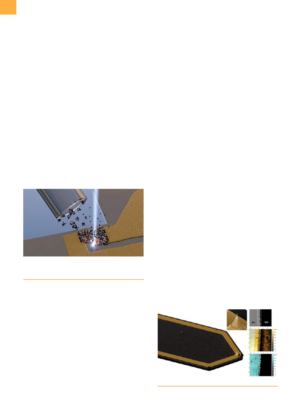
The sensor is made up of highly conductive platinum
nanoparticles surrounded by an insulating carbon matrix.
Source: EPFL
Self-sensing conductive cantilever with solid platinum tip