


 11 / 58

edfas.org
1 1
ELECTRONIC DEVICE FAILURE ANALYSIS | VOLUME 18 NO. 3
laser stimulates the region of interest, the test outcome is
compared against the reference failing signature at each
pixel. In the event of a match, a trigger pulse is gener-
ated by the comparator module and sent to the image
processor. This is how LADA signals that are not directly
relevant to the reference failing signature are negated on
the display.
HARDWARE APPROACH
Figure 2 shows a block diagram illustrating a hardware
implementation of EeLADA. As apparent in the earlier
section, the essence of the concept lies in the realizationof
the task of the comparator logic. A first-in-first-out (FIFO)
buffer array of sufficient depth functions as the memory
to capture the reference fail signature. Electrical channels
on the prober interface board that relate to the failing
pins (based on the reference fail signature) are wired
out and passed into another set of FIFO buffer arrays to
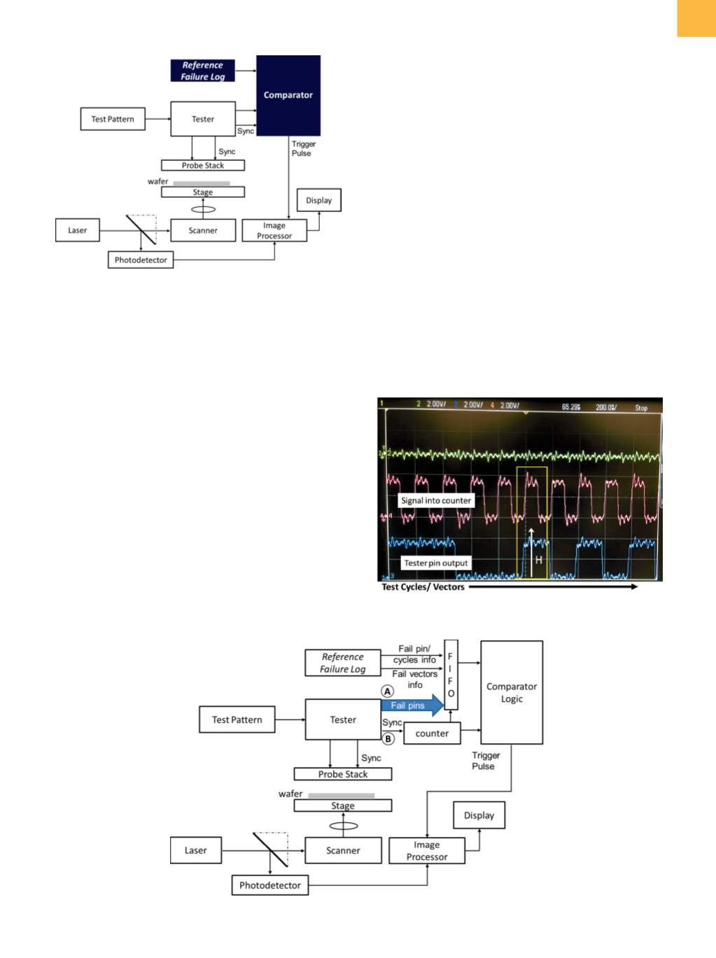
capture the pin output state at each test cycle. A pulse
that is generated by the tester within each test period
synchronizes a counter with the test cycle. The counter
increments the shifting of the FIFOarrays and coordinates
the comparator logic circuit toaccess the FIFOstates at the
failed cycles for matching. As an illustration, a passing IC
is tested, and waveforms captured at the points labeled
“A” (tester pin output) and “B” (signal into counter) are
observed on an oscilloscope. An example based on a few
test cycles is shown in Fig. 3. An instance of a test cycle is
denoted by a bounding box, and the arrow indicates the
expected compare vector (H). The output pin attains a
voltage high, which is correct.
The results of another simple experiment accom-
plished on memory built-in self-test are presented in Fig.
4. The sample under test is a good IC. Figures 4(a) and
(b) show the LADA and EeLADA signals, respectively, on
three embeddedmemory arrays. With selective pin/cycle
matching, only one of the memory arrays is revealed,
Fig. 1
Block diagram of EeLADA concept
Fig. 2
Hardware implementation of EeLADA
Fig. 3
Synchronizing signal and output pin waveforms
viewed from an oscilloscope