


 8 / 58

edfas.org
ELECTRONIC DEVICE FAILURE ANALYSIS | VOLUME 18 NO. 3
8
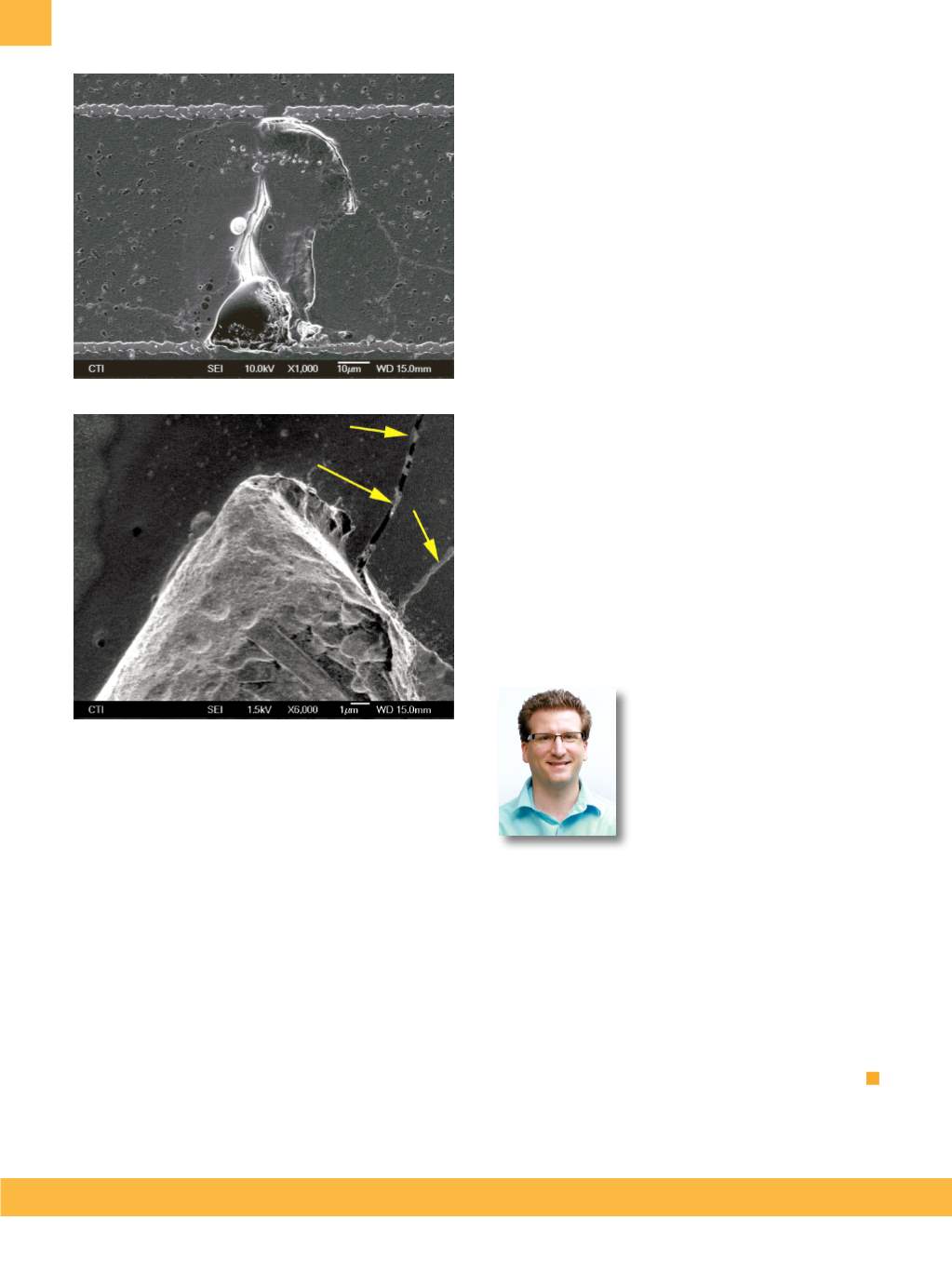
To inspect the voids at higher magnification, the SEM
was used. A detailed view of the void from the left half of
the optical view is shown in the SEM image in Fig. 6(a). In
close-up images, it can be noted that the capacitor plate
material has either melted or migrated into the air gap
in the dielectric material. As previously noted, silver—a
major component in the plates—can certainlymigrate, as
the EDS inspection showed. Both voids had a network of
fine cracks extending from the air cavity, likely induced by
expansionand contractionas thepartwas exposed tohigh
temperature during testing. Although these cracks are
small in scale, the metal from the plate material is clearly
seen filling in these cracks, as noted by the yellow arrows
in Fig. 6(b). This metal ultimately created the electrical
pathway that led to the capacitor failure.
SUMMARY
After investigating the capacitor with a variety of
methods, it was seen that internal shorting via silver
migrationwas the failuremode. It is believed that thiswas
a latent defect caused by voids in the dielectric that had
beenpresent fromthe timeofmanufacture. Through some
combination of time, electric potential, trapped humidity,
and elevated operating temperature, the plate material
migrated into these voids and created a short path to the
same floating plate. Acoustic imaging proved to be the
bestmethod for detecting the point where this failure had
occurred, although it was also clear that, in this case, a
single-pass inspection with the conventionally accepted
parameters was not able to find the voids of interest.
ACKNOWLEDGMENT
The author would like to thank his colleagues Fardin
Farzaneh, Chris Yarbrough, and Bobby Hooghan for all
their assistance.
ABOUT THE AUTHOR
John Bescup
is an electrical
engineer for Weatherford. He has
more than 10 years of failure analy-
sis experience, with an emphasis
in acoustic imaging. His day-to-
day routine includes diagnosing a
variety of nonfunctional hardware,
covering the gambit of failure analy-
sis disciplines from component-level reliability (package
and semiconductor) to board/assembly-level vibration
effects or corrosion on metal parts. John has served as
an instructor for numerous acoustic imaging training
sessions worldwide, been a tutorial session presenter
at the International Symposium for Testing and Failure
Analysis 2014-2015, andpresented at the 2016 ASMFailure
Analysis andPreventionSeminar, uponwhich this article is
partially based. He receivedhis B.S. in engineering physics
from the University of Wisconsin, Platteville in 2005.
Fig. 6
(a) SEM closeup showing a void that stretches
completely between a termination plate and a
floating plate. (b) SEM closeup with yellow arrows
highlighting metal migration within cracks that
extend from the larger void cavity between plates
(a)
(b)
Visit the Electronic Device Failure Analysis Society website edfas.org