


 6 / 58

edfas.org
ELECTRONIC DEVICE FAILURE ANALYSIS | VOLUME 18 NO. 3
6
Most capacitors use two sets of plates, withone connected
directly toeach termination. For high-voltageparts suchas
this one, manufacturers often add a third set of “floating”
plates in the center of the part that are not directly con-
nected to anything. This effectively creates two capacitors
in series. The advantage of this arrangement is a little extra
assurance that if a void or a particle of debriswere present
inside the capacitor dielectric, causinga short between the
terminationplates and thefloatingplates, therewould still
be another set of plates preventing the part from being
completely shorted. Furthermore, to create a short on a
capacitor built this way, it would be necessary for the left
set of termination plates to bridgewith the floating plates
in the center and the right-hand set of termination plates
to also be shorted with that
exact
same floating plate.
Statistically speaking, the likelihood of this scenario is
low. For this reason, the contention that this capacitor
was shorted internally because of voiding-related plate
bridging was viewed with strong skepticism.
Acousticmicroscopy is often used by capacitor manu-
facturers to screen out parts that have been compromised
by voids or debris in the dielectric material between
plates. Although air is technically an insulator, voids in
the capacitor dielectric can facilitate several failuremodes
that otherwise would not be possible. Migration of the
platemetal canoccur, as already seenon theouter surface,
and humidity can condense under the high-temperature
conditions inwhich this part will be operating. Most of the
time, ultrasonic inspection is relatively straightforward
and forgiving in the sense that even when parameters
are not perfectly optimized, it is still possible to spot any
notable defects. Among the many imaging modes avail-
able on a modern acoustic microscope, two time-tested
methods will find nearly any defect in a typical capacitor:
bulk scan and loss-of-back-echo (LOBE) scan. Because
high frequencies of ultrasound cannot propagate through
air, even incredibly small pockets of air are very effective at
reflecting an ultrasonic signal sent into the capacitor. The
LOBE technique uses this concept to advantage by depict-
ing the shadows where the ultrasonic signal was blocked
when the microscope captures a backside image of the
part. In this way, features such as diagonal cracks, which
scatter the sound without returning it to the transducer,
can still be spotted. So, the name of the imaging mode
describes exactly how it works: Any echo that is lost by the
time it reaches the back surface of the part tells the opera-
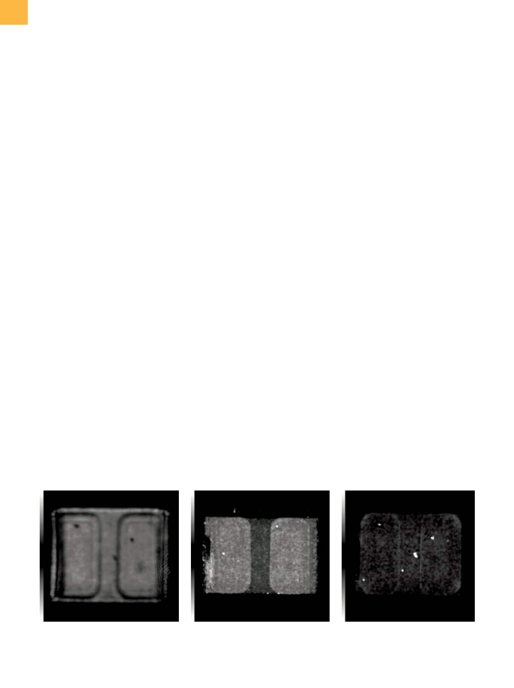
tor something. The LOBE scan in Fig. 3(a) shows a fewdark
areas, which can be checked against forthcoming scans.
The other main inspection method used to search for
defects in cap dielectric is bulk scan, where the image
is generated by only those reflections originating from
inside the part, purposely excluding the front and back
surface reflections. In this imaging mode, bright reflec-
tions represent air gaps inside the bulk of the dielectric.
Figures 3(b) and (c) show two bulk scans of the shorted
capacitor. When creating these images, the transducer
is typically focused halfway between the front and back
surface, which, in this case, was measured to occur at
a time of flight (TOF) equal to 13.9 µs. However, when
this accepted convention is used, the resultant image
shows no voids at the locations indicated by the LOBE
scan. After repeating the scan with a higher and lower
TOF, the operator discovered that different sets of voids
were revealed, depending on the transducer focus. The
particular combination of materials used in this dielectric
material is restricting the acoustic depth of field. This is
not normally the case, and it gives a plausible reasonwhy
acoustic inspection at the time of manufacture may have
missed a set of voids that did not appear when the acous-
tic microscope was configured according to customary
settings for bulk scan inspection. The image in Fig. 3(c),
which was created with a TOF equal to 10.2 µs, reveals
Fig. 3
(a) LOBE acoustic image. (b) Bulk scan acoustic image with TOF at 13.9 µs. (c) Bulk scan acoustic image with TOF at
10.2 µs
(b)
(a)
(c)