


 5 / 58

edfas.org
5
ELECTRONIC DEVICE FAILURE ANALYSIS | VOLUME 18 NO. 3
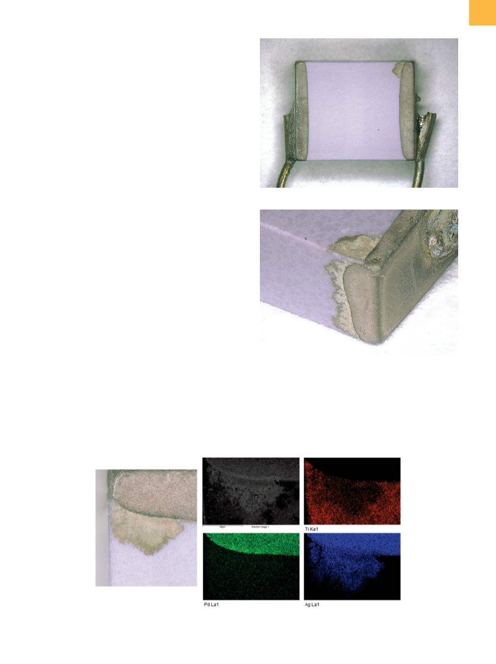
determine the nature of the dendritic growth, energy-
dispersive spectroscopy (EDS) was performed. By creating
the series of element maps shown in Fig. 2, it was deter-
mined that silver had migrated onto the capacitor face.
The other principal component of the termination mate-
rial, palladium, had remained completely in place. As
foreshadowing, note that the internal capacitor plates
also contain silver.
While the capacitor was in the scanning electron
microscope (SEM) chamber, elemental quantification
data were also gathered on the solder to verify that it had
the intended composition. Because components in the
oil-drilling industry are pushed into very extreme operat-
ing environments, a restriction of hazardous substances
exception allows these boards to use leaded solder. A
rectangular-area EDS spectrum acquired over the discol-
oredareawhere the lead joins the cap termination showed
75/23 lead/tin, with the balance being silver. This is a
close-enough match to the expected composition to rule
out the possibility that the solder joint had been contami-
natedwith a low-temperature solder duringmanufacture.
Because component andPCBmanufacturerswho provide
high-temperature assembly always offer low-temperature
products as well, the possibility of inadvertently mixed
solder alloys is a constant threat to reliability thatmust be
guarded against. Consulting the tin-lead phase diagram,
the liquidous point of 75% lead solder is just above
500 °F, soour termination certainly experienced some heat
in order to discolor and partially reflow.
NONDESTRUCTIVE INTERNAL
ANALYSIS
Before going further, it is necessary to understand a bit
more about the constructionof this particular component.
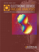
Fig. 1
(a) Optical image showing overall view of the failed
capacitor. Note dendrite growth at upper right and
the reflowed termination solder with heat-stress
discoloration on the right side. (b) Closeup of
dendritic growth from termination onto the cap face
(a)
(b)
Fig. 2
EDS mapping of the dendrite growth. Starting at top-middle image and going clockwise: SEM grayscale image, red
titaniummap, blue silver map, green palladiummap, and color optical image