


 16 / 54

1 6
LASER ANNEALING ENABLES
ULTRATHIN NANOMATERIALS
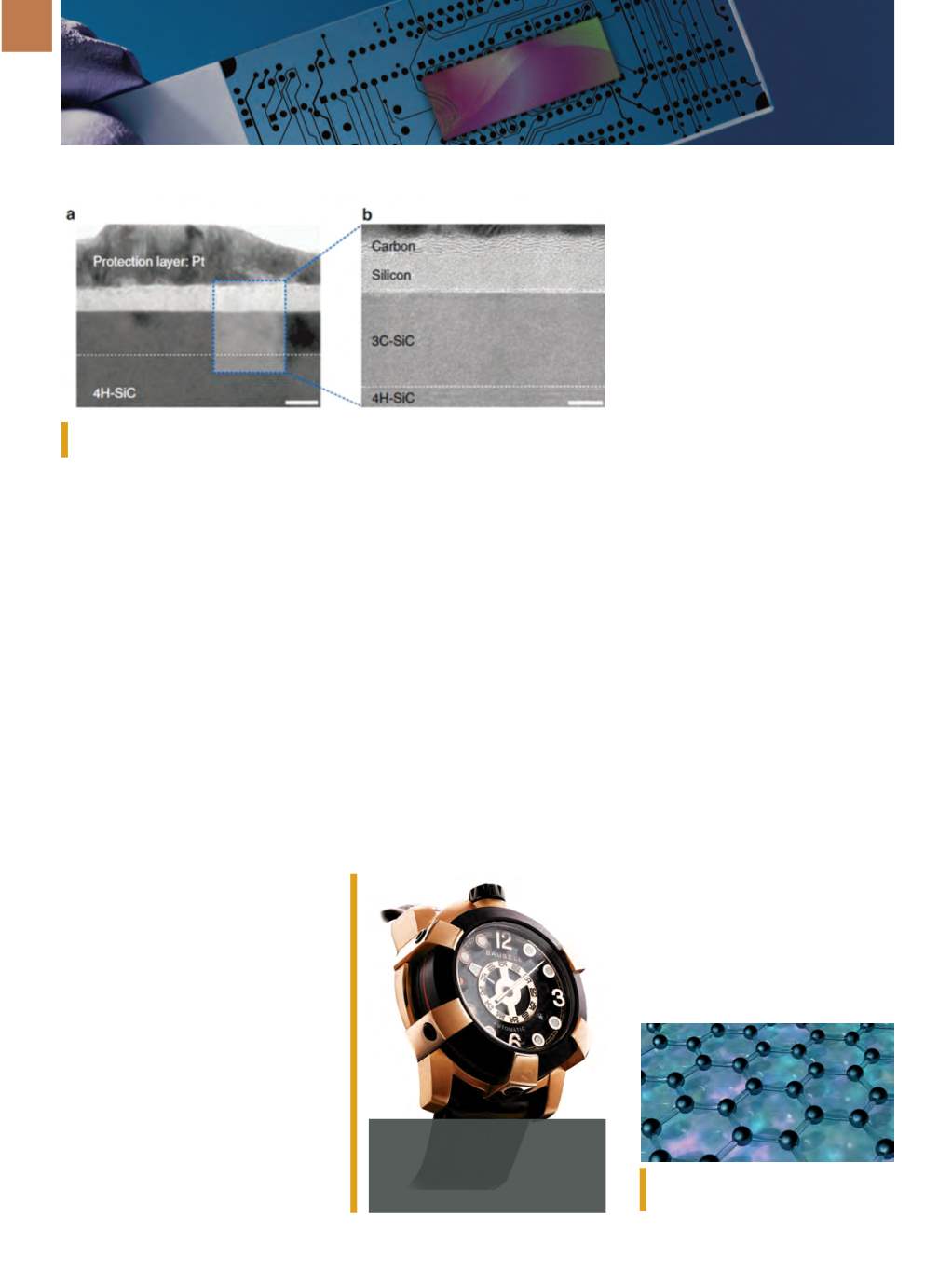
Researchers at the Institute for
Basic Science, together with a team
at KAIST, both in South Korea, discov-
ered a graphene synthesis mechanism
using laser-induced solid state phase
separation of single-crystal silicon car-
bide (SiC). Their research clarifies how
this laser technology can separate a
complex compound (SiC) into its ultra-
thin elements. Using high resolution
microscope images and molecular dy-
namic simulations, scientists found
that a single-pulse irradiation of xenon
chloride excimer laser of 30 ns melts
SiC, separating a liquid SiC layer, a dis-
ordered carbon layer with graphitic
domains (about 2.5 nm thick) on the
top surface, and a polycrystalline sil-
icon layer (about 5 nm) below the car-
bon layer. Additional pulses cause the
sublimation of the separated silicon,
while the disordered carbon layer is
transformed into multilayer graphene.
www.ibs.re.kr/eng.do,kaist.edu.
WATCH NEW CERAMIC NANO-
TECHNOLOGY IN ACTION
A new watch from Bausele Aus-
tralia uses an innovative material called
Bauselite developed in partnership with
Flinders University’s Centre of NanoScale
Science and Technology, Australia. The
advanced ceramic nanotechnology is
featured in the company’s Terra Australis
watch. Apart from the face, the case is the
most prominent featureonawatchhead—
so it needs to be visually appealing but
also lightweight and strong, says company
founder Sydneysider Christophe Hoppe.
Using a new technique, the teamcreated a
ceramic-likematerial that canbeproduced
in small batches via a non-casting pro-
cess, which helps eliminate defects found
in conventional ceramics. “Bauselite is
strong, very light and, because of the way
it is made, avoids many traps common in
conventional ceramics,” explains Hoppe.
The new material also allows holes to be
drilled more precisely. “It means we can
make bolder, more adventurous designs,”
he adds.
bausele.com.
After just one 30-ns laser pulse, an SiC substrate is melted and separates into a carbon
and a silicon layer. Courtesy of IBS.
2DMATERIALS ENHANCE
ELECTRONIC DEVICES
A new study by an international
team of researchers led by the Universi-
ty of Minnesota, St. Paul, highlights how
manipulating 2D materials could make
modern day devices faster, smaller, and
more efficient. Researchers examined
the optical properties of dozens of 2D
materials to unify understanding of
light-matter interactions and explore
possibilities for future research. They
found that polaritons—a class of quasi-
particles formed through the coupling
of photons with electric charge dipoles
in solid—allow the marriage of photon
light particle speed with the small size
of electrons. “With our devices, we want
speed, efficiency, and we want small.
Polaritons could offer the answer,” says
Tony Low, assistant professor of elec-
trical and computer engineering. By
exciting the polaritons in 2D materials,
electromagnetic energy can be focused
down to a volume a million times small-
er compared to when it is propagating
in free space.
“Layered 2D materials have
emerged as a fantastic toolbox for
nanophotonics
and
nanooptoelec-
tronics, providing tailored design and
tunability for properties that are not
possible to realize with conventional
materials,” explains Low.
For more in-
formation: Tony Low,
tlow@umn.edu,
twin-cities.umn.edu.
NANOTECHNOLOGY
Each timepiece features red earth from
the Outback, beach sand, or opal—
allowing wearers to take a piece of
Australia with themwherever they go.
2Dmaterials allow strong light-matter
interactions through polaritons.
A D V A N C E D M A T E R I A L S & P R O C E S S E S | J A N U A R Y 2 0 1 7