


 23 / 78

A D V A N C E D
M A T E R I A L S
&
P R O C E S S E S | J A N U A R Y
2 0 1 6
2 3
thermal grease, effectively doubling the
thermal barrier problem.
In CPUs, and also inmany through-
hole and surface-mount devices, it is
necessary to connect the electrical
component to other components, gen-
erally through a printed circuit board
(PCB). The components experience
heating when they are soldered to a
PCB or require very precise wire bond-
ing or flip chip equipment, which often
demands a thermosonic bonding meth-
od. In some cases, temporary heat sinks
must be attached to the component
during soldering to prevent damage
[9]
.
Also, as component size decreases, sol-
dering or wire bonding becomes more
challenging and voids can lead to joint
failure
[10]
. A metallic glue bond elimi-
nates the possibility of heat damage
during attachment and simplifies the
soldering process to merely pressing
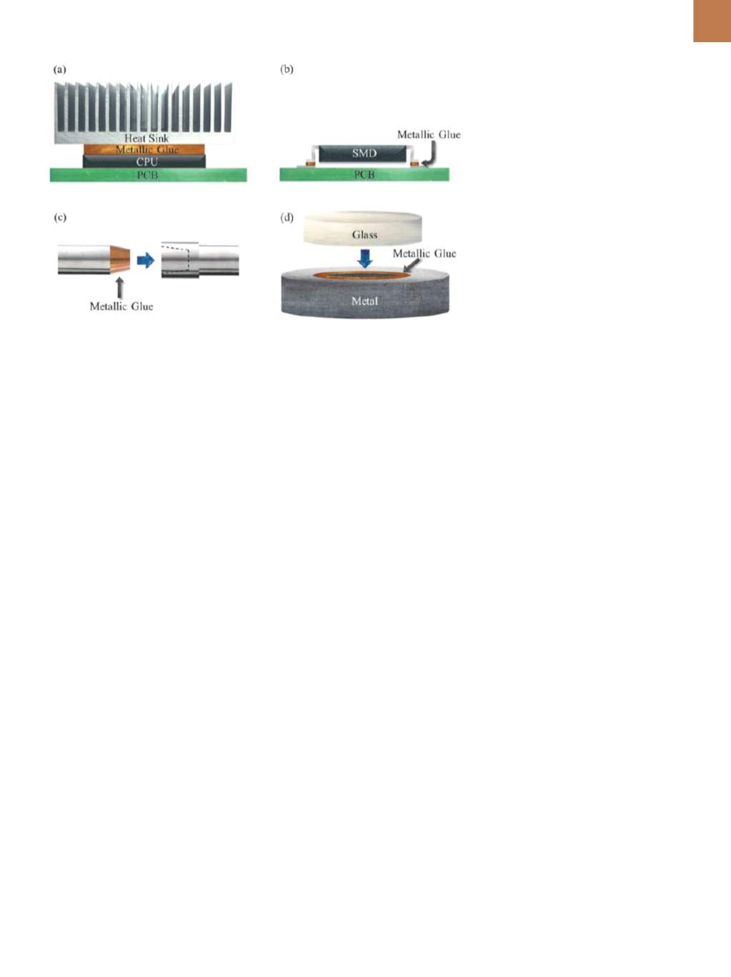
parts together to attach (Fig. 1b).
A third example involves connect-
ing pipes or construction parts togeth-
er, which highlights the benefits of the
metal bond’s strength (Fig. 1c). Withme-
tallic glue, no gases, electricity, or heat
is required. This facilitates a process
that poses zero risk of asphyxiation,
electric shock, or burns, and occurs in
safe environments where welding may
not be safe or possible, such as hot
work in confined spaces. In addition, no
welding skill is required.
As a fourth example, the hermetic
sealing of materials with much different
coefficients of thermal expansion (CTE)
benefits greatly from a room tempera-
ture bonding method. Generally, when
sealing metal to ceramic or glass, ma-
terials must be carefully selected to
have a similar CTE. If the CTE difference
is too large, parts may separate due
to geometric mismatch when cooled.
When selection of similar CTE materials
is not possible, part geometry must be
carefully designed so that thermally in-
duced stresses do not become too large
to cause warping or material failure.
Application examples include compact
fluorescent bulbs, glass encapsulated
diodes, and windows for inspection and
diagnostics in industrial processes and
vacuum chambers (Fig. 1d).
NANOSCIENCE-ENABLED
TECHNOLOGY
Combining the ambient condi-
tions of gluing with the desirable prop-
erties of soldering would be possible
if one could use metal as solder at
room temperature. Until recently, this
remained wishful thinking based on
Fig. 1 —
Various applications of metallic glue: (a) A central processing unit (CPU) on a printed
circuit board (PCB) connected to a heat sink, (b) a surface mount device attached to a PCB, (c) a
press-fit pipe fitting for environments where welding is dangerous or impossible, and (d) a glass
plate attached to metal with a different coefficient of thermal expansion to cover a cavity with a
hermetic seal.
conventional technologies. Now, ad-
vancements in both science and tech-
nology have made this sought-after
ability a reality
[11]
. Figure 2 outlines a
new process that uses nanostructures
and eutectic alloys to produce a room
temperature metallic glue with the de-
sirable properties of solder. In Fig. 2a,
two surfaces to be bonded together are
shown facing one another. Each surface
is covered with core-shell nanorods.
When the mating surfaces are brought
together, the large spacing of the na-
norods allows them to slide between
those on the opposing surface and to
interpenetrate (Fig. 2b). When the shell
materials from opposing sides come
into contact, which together form an
alloy with a eutectic temperature at or
below room temperature, a liquid alloy
is quickly formed (Fig. 2c). Interdiffu-
sion between the liquid alloy and the
nanorod cores leads to solidification as
the composition deviates from that of
eutectic alloys of low melting tempera-
ture (Fig. 2d).
Development of this emerging
technology is based on efforts to un-
derstand how and why nanostructures
grow at a fundamental level. One im-
portant subject of investigation in na-
noscience has been nanorod growth
using glancing angle physical vapor
deposition
[12]
. A recent breakthrough
in this field involves the development
of a theory for both the diameter and
separation of nanorods
[13,14]
. Guided by
this theory, the smallest, well separated
metallic nanorods came to light (Fig. 3).
Developing the ability to produce
well separated nanorods is an import-
ant step in realizing this technology,
due to the necessity of interpenetra-
tion of the nanorods. If they are not
sufficiently well separated, the rods
will contact one another head-on and
act like a porous film. Consequently,
bonding will not be successful at low
temperatures
[15]
. At this small scale,
if the separation is sufficient, a small
shear stress will align the nanorods for
inter-digitation, even if they are not well
aligned upon initial contact. Further, at
the small diameter, a new mechanism
of surface diffusion becomes active,