


 31 / 102

A D V A N C E D
M A T E R I A L S
&
P R O C E S S E S |
O C T O B E R
2 0 1 5
3 1
how hot the area is and where the pow-
er dissipation occurs in the logic block.
Another defect localization tech-
nique is light emission microscopy, also
known as EMMI. It can be used from
either the front or back of the die (of-
ten without die thinning) to discover
defects or abnormal device operation
based on photon emission in the vis-
ible and near-infrared (IR) spectrum.
These defect-related emissions are of-
ten associated with forward or reverse
biased p-n junctions. In the example of
forward-biased p-n junctions, device
emission is generated by placing a large
number of electrons and holes in close
physical proximity where they recom-
bine and generate light with spectra
centered around the silicon bandgap.
This light can be captured with a sensi-
tive charge-coupled device (CCD) or in-
dium gallium arsenide (InGaAs) camera
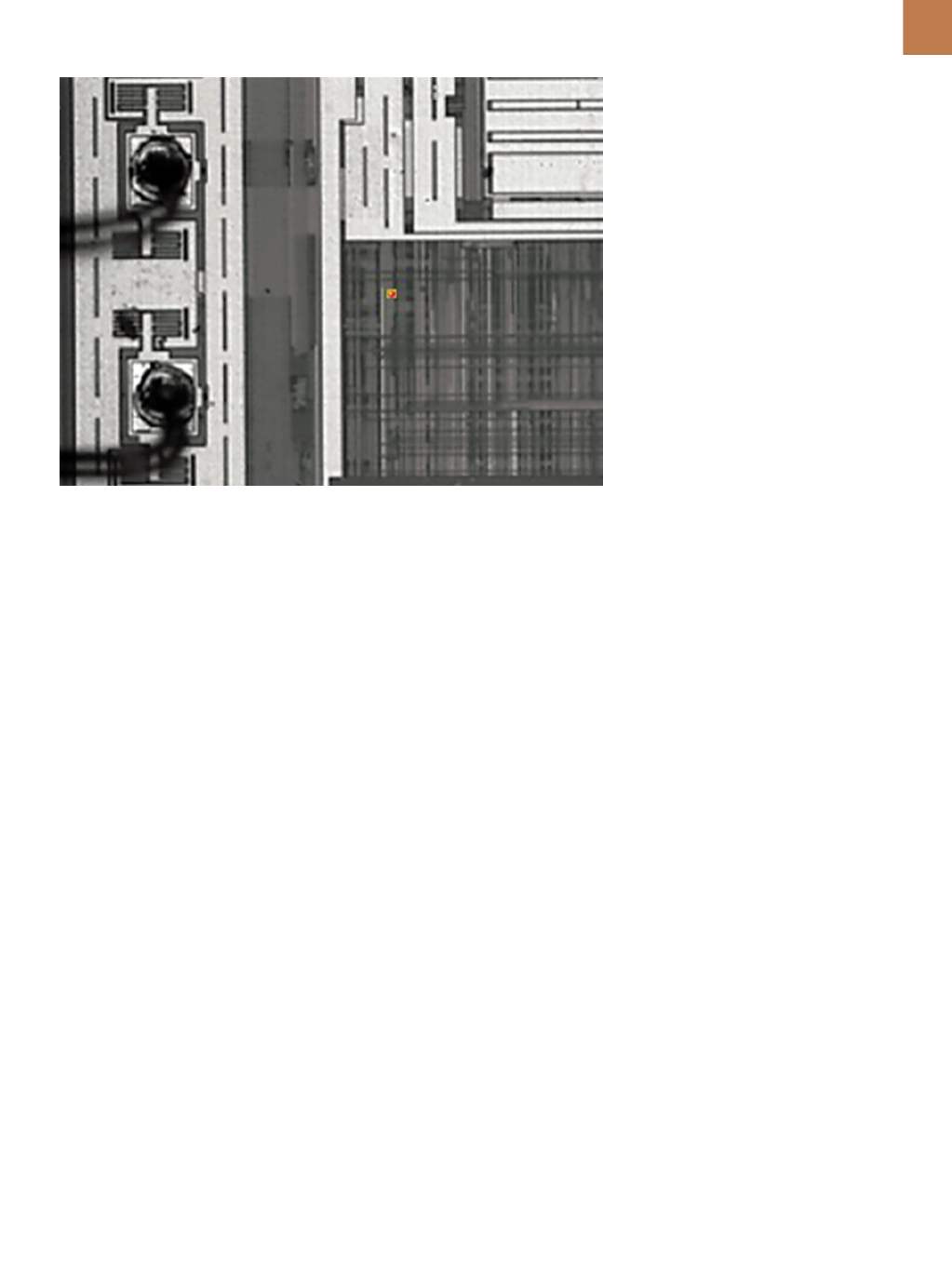
in a light-tight box. Two images are cap-
tured, one with the microscope light on
to acquire the die image, the next with
the light off and bias applied to see the
emission source (Fig. 4).
Defect-related photon emissions
are also generally associated with tran-
sistors in saturation, latch-up, and gate
oxide breakdown. In avionics applica-
tions, these types of failures can be the
result of single event effects (SEE), a
category of isolated electronic circuitry
changes resulting from interactions with
high-energy particles and radiation in
space. For instance, a single event latch-
up (SEL) can cause a transistor element
to become fixed in either an on or off
state, or a memory bit to become stuck
at either a one or zero, latching the ef-
fected cell into a permanent state. Latch-
ups, in particular, shine very brightly
using light emission microscopy. Re-
gardless of device type, any transistor
under normal operation will generate a
small amount of light. All light emission
sites are overlaid on a background die
image, enabling failure localization in
relation to circuit features.
Laser signal injection microscopy is
another important imaging tool, and is
used to locate IC defects such as shorts,
junction defects, and problems with
vias. A laser beam is scanned through
a microscope lens over the die while
watching for laser-induced shifts in the
device current-voltage (I-V) response.
Short-wavelength lasers inject photo-
currents and can reveal failure sites
in transistors and p-n junctions, while
longer-wavelength lasers create local-
ized heating that results in temporary re-
sistance changes. In the latter example,
leakage paths can be revealed due to the
temperature coefficient of resistance.
It is also useful to look at the re-
flected laser light image and its am-
plitude using laser timing probe (LTP)
techniques. Because the brightness of
the reflected laser changes with the volt-
age on the transistor, an individual tran-
sistor’s waveform can be measured by
running a logic pattern through the sam-
ple. It is also possible to see what is not
switching, as well as locations that are
switching at a certain clock or data fre-
quency, or where a clock stops halfway
through, helping to localize the defect.
Localizing failures at the transis-
tor level may also require nanoprobe
techniques. Polishing the sample expos-
es contacts, and a biased probe tip is
scanned across its surface to reveal sub-
tle leakage differences between sources,
drains, and gates. Another option is to
drop up to six probes onto the transistor,
make contact at the source, gate, drain,
and body, and measure the electrical
characteristic of each individual tran-
sistor. Electrical characteristics such as
threshold voltage, off leakage, and on
current can then be measured. Once the
problem transistor has been identified,
physical analysis can take place.
Transmission
electron
micro-
scopes (TEMs) are often used after
nanoprobe tests. Samples are placed
under a focused ion beam and trenches
are dug on each side of the target tran-
sistor, leaving only a slice the size of the
transistor itself. This slice is viewed un-
der the TEM to visualize defects in a way
that no other technology can.
Avionics system failures are diffi-
cult to identify and solve. The combina-
tion of smaller and more complex de-
vices used in demanding environments
makes it difficult to find and fix failures.
Identifying, localizing, and resolving
failures requires a highly disciplined
process, supported by numerous so-
phisticated test and imaging tools. With
the right approach, it is possible to iso-
late a failure’s root causes, understand
its mechanisms, and resolve it.
~AM&P
For more information:
Winfield Scott
is technology director, Evans Analytical
Group, 2710 Walsh Ave., Santa Clara, CA
95051, 408.454.4600,
wscott@eag.com,
www.eag.com/mte.Fig. 4 —
Emissionmicroscopy requires little or no sample preparation, other than decapsulation.