


 30 / 102

A D V A N C E D M A T E R I A L S & P R O C E S S E S | O C T O B E R 2 0 1 5
3 0
across adjacent conductors and, at high
altitudes, these shorts can result in con-
ductive plasma generation.
Other nondestructive tests include
a superconducting quantum interfer-
ence device (SQUID) and giant magne-
toresistive (GMR) microscopy. Both are
magnetic current imaging tools useful for
finding shorts and leakages, and map-
ping their locations on the current path.
Thermal imaging can also be used to
identify and map hot spots and provide
actual temperature measurements. An-
other common nondestructive electrical
test is curve trace. Voltage and current
are swept to create an I-V plot, which re-
veals opens and shorts as well as resis-
tance and leakage, helping to verify and
visualize the electrical failure signature.
Nondestructive package tests in-
clude particle impact noise detection
(PIND) for cavity packages, which is es-
sentially a process of shaking the sam-
ple and listening for loose particles in-
side. Fine and gross leak tests are both
used for evaluating hermetic package
integrity. In addition, 2D or 3D x-ray
imaging is useful for analyzing package
integrity and provides a look at PCB in-
ternal traces, bond wires, die bumps,
de-attached fillets, substrate package
traces, and other package elements.
Scanning acoustic microscopy (SAM)
uses ultrasound pulse echo techniques
to look for voids, cracks, and delamina-
tions in ceramic capacitors and plastic
packages. Also, TDR can be used here to
help determine whether an open/short
defect is in the package or at the inter-
face to the die. Other nondestructive
optical tests include filtered polarized
light inspection, as well as die backside
inspection using reflected IR imaging.
Based on the electrical failure sig-
nature and initial nondestructive test-
ing results, a plan for physical analysis
can be formulated. At this point, inter-
nal visual inspection using low- and
high-magnification optical microscopy
is often used to further localize the prob-
lem. Optical and scanning electron mi-
croscope (SEM) inspection can also help
analysts understand morphology and
electrostatic discharge (ESD) issues, and
can be combined with materials charac-
terization tests to identify foreign ma-
terials or corrosive byproducts such as
chlorine that would indicate problems
related tomoisture infiltration.
Rounding out the options for
package testing are backside infrared
(IR) thermography and other back-
side laser inspection techniques, and
cross-sectioning to look at joint profiles
with SEM and other higher-resolution
instruments.
LOCALIZING FAILURES TO
THE TRANSISTOR LEVEL
Once an electrical failure has been
identified through nondestructive test-
ing, the failure mechanism must then
be localized to within a few microns of
the problem’s exact location. Analysts
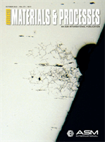
use optical microscopy to look at bond
wires, die attach, big cracks in the die,
electrical overstress, corrosion, and
other large elements on the die. Wire
bonds are a particularly vulnerable de-
sign element in avionics systems, which
are prone to intermetallic formation due
to exposure to elevated temperatures,
corrosion due to both high temperature
and moisture, and fatigue due to tem-
perature cycling exposure (Fig. 2).
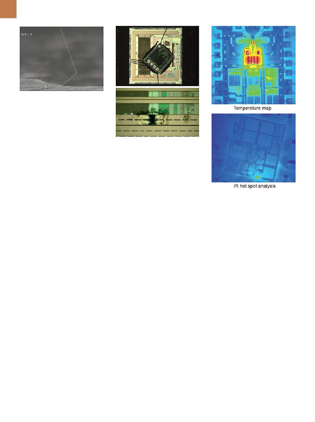
Infrared thermography is another
important technique. Avionics packages
are frequently exposed to temperatures
higher than the maximum allowable for
their electronics, reducing component
lifetimes and significantly increasing
failure probability. Infrared thermog-
raphy microscopes localize hot spots
by measuring true temperature with
pixel-by-pixel emissivity correction.
Heat is imaged at a 3-micron infrared
wavelength to create a color-coded tem-
perature map or hot spot overlay image.
Figure 3 shows two examples
where power was dissipated in the sam-
ple and creating hot spots. Temperature
increase depends on the power dissi-
pated per unit area, so in this case iden-
tifying where the device was getting hot
is easy. Infrared thermography indicates
Fig. 1 —
Scanning electron microscope
image of tin whiskers.
Fig. 2 —
Low- and high-magnification
microscopes can be used to visualize a
package’s wires and wire bonds, passivation
cracks, electrical overstress, and corrosion.
Fig. 3 —
Temperature gradient across the
die, top, and location of a gate oxide break-
down site, bottom.