


 11 / 78

ADVANCED MATERIALS & PROCESSES •
NOVEMBER-DECEMBER 2014
11
news
industry
briefs
I
n October,
The Boeing Co.
celebrated the groundbreaking of
its 777X Composite Wing Center in
Everett, Wash. Permitting for the
new 1-million-sq-ft facility was
completed approximately seven
weeks early. The new building is
expected to open in May 2016
with the first 777X delivery
targeted for 2020. To date, 300
orders and commitments have
been received. Two models will
comprise the new family—the
777-8X, with 350 seats and a
range of more than 9300 nautical
miles, and the 777-9X, with 400
seats and a range of more than
8200 nautical miles.
boeing.com.
President Barack Obama
announced an upcoming
competition, sponsored by the
U.S.
Department of Defense (DoD),
that will provide an award of up to
$110 million in federal funds to
launch an
Institute for
Manufacturing Innovation (IMI)
whose work involves photonics.
The
Integrated Photonics IMI
is
the fourth DoD-led manufacturing
institute to be announced since
the pilot project was launched in
August 2012. Beginning early this
month, the DoD will collect
proposals from teams of nonprofit
organizations, universities, and
private companies to head the
institute. The $110 million
available over five years must be
matched by at least $110 million
in nonfederal commitments.
defense.gov.Physicists at the DOE’s Ames
Laboratory developed the first
model of a photonic band-gap
crystal. Courtesy of U.S.
Department of Energy.
P
ROCESS
T
ECHNOLOGY
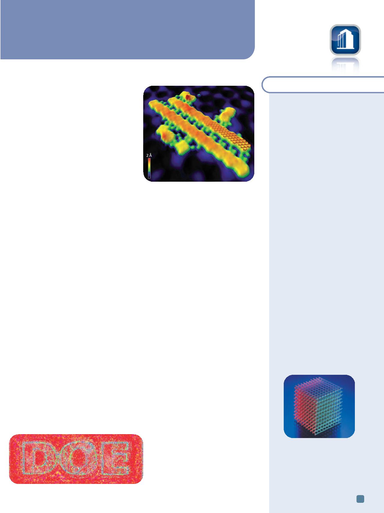
Self-assembly method promises perfect graphene
Scientists fromUniversity of California,
Los Angeles (UCLA) and Tohoku Univer-
sity, Japan, discovered a new self-assembly
method to produce defect-free graphene
nanoribbons with periodic zigzag-edge re-
gions. In this bottom-up technique, a cop-
per substrate’s unique properties are used to
change the way the precursor molecules
react to one another as they assemble into
graphene nanoribbons. This allows scien-
tists to control the ribbons’ length, edge
configuration, and location on the substrate.
Researchers say the new method of
graphene fabrication by self-assembly is a
stepping stone toward production of self-
assembled graphene devices that will vastly
improve the performance of data storage
circuits, batteries, and electronics. Paul Weiss, distinguished professor of chemistry and
biochemistry and a member of UCLA’s California NanoSystems Institute, developed the
method for producing the nanoribbons with Patrick Han and Taro Hitosugi, professors at
the Advanced Institute of Materials Research at Tohoku University in Sendai, Japan.
cnsi.ucla.edu.
New process controls properties of 3D printed metal parts
Researchers at DOE’s Oak Ridge National Laboratory (ORNL), Tenn., demonstrated
an additive manufacturing method to control the structure and properties of metal com-
ponents with precision that is reportedly unmatched by conventional manufacturing
processes. Ryan Dehoff, staff scientist and metal additive manufacturing lead at ORNL’s
Manufacturing Demonstration Facility, presented the research in an invited presentation
at the Materials Science & Technology 2014 conference in Pittsburgh, in October.
“We can now control local material properties, which will change the future of how we
engineer metallic components,” says Dehoff. “This new manufacturing method takes us
from reactive design to proactive design. It will help us make parts that are stronger, lighter,
and function better for more energy-efficient transportation and energy production appli-
cations such as cars and wind turbines.”
Researchers demonstrated the method using an ARCAM electron beam melting sys-
tem (EBM), in which successive layers of a metal powder are fused together by an electron
beam into a 3D product. By manipulating the process to precisely manage solidification on
a microscopic scale, scientists demonstrated 3D control of the microstructure of a nickel-
based part during formation. Applications from microelectronics to high-temperature jet
engine components rely on tailoring of crystallographic texture to achieve desired per-
formance characteristics.
“We’re using well established metallurgical phenomena, but we’ve never been able to
control the processes well enough to take advantage of them at this scale and at this level
of detail,” explains Suresh Babu, the University of Tennessee-ORNL Governor’s Chair for
Advanced Manufacturing. “As a result of our work, designers can now specify location-
specific crystal structure orientations in
a part.”
ornl.gov.Electron backscatter diffraction image
shows variations in crystallographic
orientation in a nickel-based component,
achieved by controlling 3D printing at the
microscale. Courtesy of ORNL.
Graphene nanoribbons imaged by scanning
tunneling microscopy. Zigzag edges are
highlighted by the red structure. Courtesy of
Patrick Han.