


 42 / 62

 edfas.org
ELECTRONIC DEVICE FAILURE ANALYSIS | VOLUME 18 NO. 1
42
PRODUCT NEWS
Larry Wagner, LWSN Consulting Inc.
lwagner10@verizon.netPRESS RELEASE SUBMISSIONS:
MAGAZINES@ASMINTERNATIONAL.ORGFEI ANNOUNCES HELIOS G4 DUALBEAM
FEI (Hillsboro, Ore.) announced the new Helios G4
DualBeam series, which offers the highest-throughput
ultrathin transmission electron microscopy (TEM) lamella
preparation for leading-edge semiconductor manufactur-
ing and failure analysis applications. The new DualBeam
series, which includes FX andHXmodels, takes a significant
leap forward in both technological capability and ease of
use.
The new Phoenix focused ion beam makes finer
addition, by offering the ability to achieve sub-3 Å image
resolution in a DualBeam, failure analysis labs can now
dramatically cut time to datawithout compromising image
quality. And, by combining high-resolution imaging and
sample preparation on one system, we have reduced the
amount of valuable lab real estate required.”
For more information: web:
fei.com; tel: 408.224.4024.
DCG INTRODUCES MERIDIAN M
DCG Systems (Fremont, Calif.) announced the release
of the Meridian M system for isolation of routine and chal-
lenging electrical faults at the wafer level. Offering photon
emission for transistor-level defects and leakage and a
complete portfolio of static laser simulation techniques for
metallization defects, the Meridian M system is a critical
tool to support production-use cases in memory and
foundry failure analysis labs. Its high-sensitivity, extended-
wavelength DBX optics capture even themost challenging
faults, including:
• Large-area process variation in advanced memory
devices that can lead to anomalous leakage
• High-resistivity wordline-to-wordline or bitline-to-
bitline shorts within memory cells
• Resistive faults in low-voltage graphics processing units
and other low-voltage logic circuits
• Any weakly emitting faults requiring long integration
time
The Meridian M system also captures electrical
faults that emit photons primarily in the thermal range
(>1850 nm), such as partial opens, high-ohmic shorts, and
electromigration.
“Static optical fault isolation (OFI) is in a renaissance,”
said Praveen Vedagarbha, business unit manager of the
Meridian Product Group at DCG Systems. “While dynamic
OFI is important for localizing parametric faults, static OFI
is faster and easier to use than its dynamic counterpart
because it does not require docking to a tester or having
the device and tester knowledge necessary to edit the
test program. The speed and ease of use of the Meridian M
system is particularly valuable in early yield ramp, when
rapid feedback to the process engineering team is critical.”
cuts with higher precision and simplifies the creation of
ultrathin (sub-10 nm) lamella for TEM imaging. The FX
is a flexible system that delivers dramatically improved
scanning transmission electronmicroscopy (STEM) resolu-
tion—down to sub-3 Å—and significantly shortens the time
to data for failure analysis. Images can now be obtained
within minutes of completing the lamella, rather than the
hours or days previously required to finalize the images
on a stand-alone S/TEM system. The HX model is geared
specifically for high-throughput TEM lamella production.
It features an automated QuickFlip holder that reduces
sample preparation times.
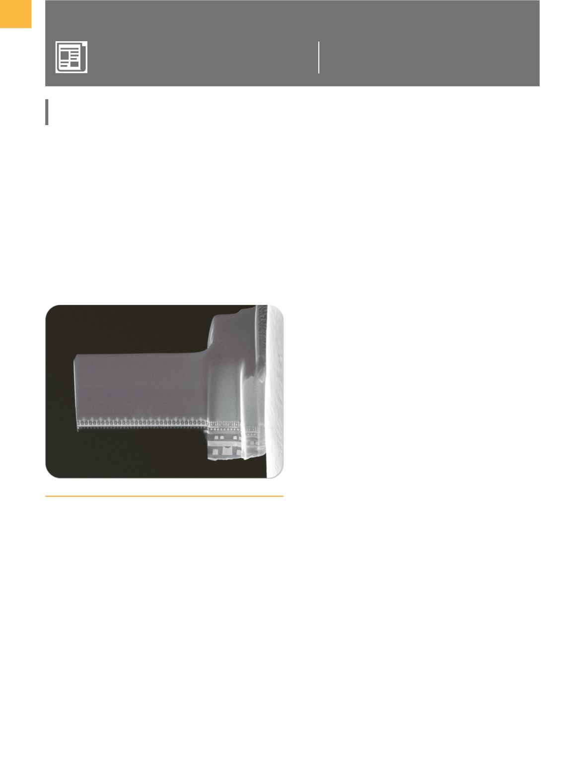
“FEI is thefirst tomarketwithaTEMsample-preparation
solution capable of making 7-nm-thick lamella, addressing
the needs of our customers who are developing next-
generation devices,” states Rob Krueger, Vice President
and General Manager of FEI’s semiconductor business. “In
Inverted lamella