


 43 / 62

 edfas.org
43
ELECTRONIC DEVICE FAILURE ANALYSIS | VOLUME 18 NO. 1
Visit the Electronic Device Failure Analysis Society website
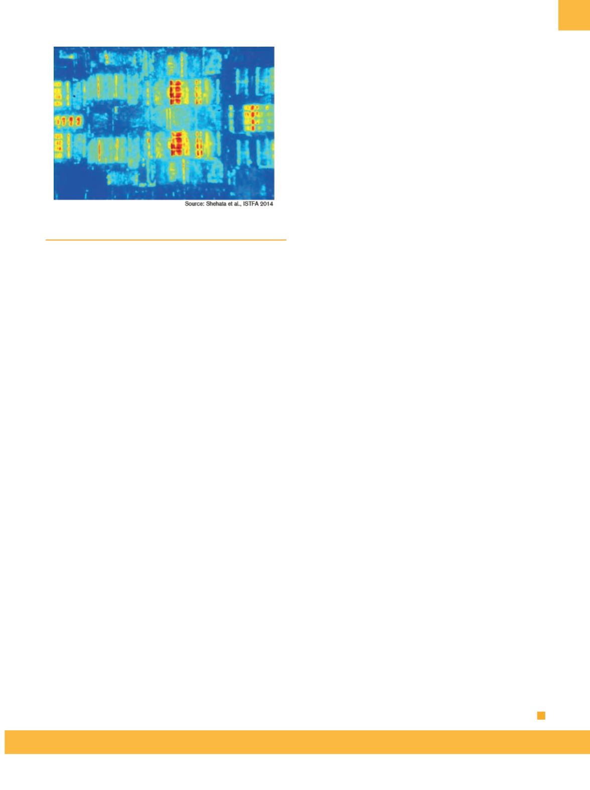
edfas.orgAmong static-only OFI systems, Meridian M has dem-
onstrated superior performance in localizing faults with
the weakest photon emission. Custom-designed optics, a
set of user-selectable wavelength ranges, and the lowest
background noise in the industry allow Meridian M to be
optimized for a variety of fault types, from conventional
“optical” emitters such as excessive leakage, saturation,
and latch-up faults to longer-wavelength “thermal”
emitters, such as high-resistance shorts and dopant dis-
placement errors. Because it accommodates full wafers
in addition to packaged die, the Meridian M system allows
comparison of good die to bad die, aiding interpretation of
complex thermal and photon emission images.
The Meridian product line at DCG Systems leads the
industry in active installed base, with wafer-based or
packaged-part systems at all leading fabless, foundry, and
integrated device manufacturers.
For more information: web:
dcgsystems.com/ products/electrical-fault-analysis/meridian-line/ meridian-m/;e-mail:
jet_perland@dcgsystems.com.
RENISHAW OFFERS inVIA CONFOCAL
RAMAN MICROSCOPE
Renishaw (Gloucestershire, U.K.) is an experienced sup-
plier of integrated Raman-atomic force microscopy (AFM)
solutions, having offered them for more than 16 years.
The latest addition to the range of instruments it supports
is Bruker’s Dimension Icon AFM. This additional pairing
demonstrates the extreme flexibility of the Renishaw inVia
confocal microscope and its capability to interface with
a wide range of instruments employing many analytical
techniques.
The inVia-Icon is a fully integrated Raman-AFM system.
It has a comprehensive range of features, making it the
highest-performing yet easy-to-use system for co-localized
Raman-AFMmeasurements. It supports a full range of AFM
techniques and µ-Raman capabilities and can characterize
the properties of materials at submicrometer and nano-
meter scales.
The Dimension Icon provides users with uncompro-
mised performance, robustness, and the flexibility to
perform nearly every AFM measurement type at resolu-
tions previously only obtained by extensively customized
systems. The inVia microscope complements this by pro-
ducing both rich, detailed, chemical images and highly
specific Raman data from discrete points. Users can make
both Raman and AFMmeasurements withoutmoving their
samples between instruments andwithout compromising
performance. In addition, both instruments can be used
independently, if necessary.
The inVia-Icon combination has a flexible arm linking
the two instruments; this couples light between the two
with mirrors, providing a higher efficiency than fiber optic
coupling. This ensures that users can acquire high-quality
data in the minimum time with market-leading signal-to-
noise levels.
The flexible coupling arm employs Renishaw’s
StreamLineHR high-resolution mapping technology. It
can Raman map areas up to 500 µm
×
500 µm, with posi-
tion encoders ensuring 100 nm repeatability. Bruker’s
proprietary PeakForce QNM complements StreamLineHR
by providing even higher-resolution nanomechanical
information.
“Renishaw’s patented sampling armallows the sample
to bemeasuredwhile it is still mounted on the AFM. Making
correlated measurements with both systems is easy,” said
Tim Batten, Renishaw applications scientist. He added,
“The arm does not contact the AFM and, as such, does not
affect its performance.”
Adding inVia’s powerful chemical imaging capabilities
to the Bruker Dimension Icon sets a new standard, deliver-
ing high-performance surface characterization with both
efficiency and ease.
For more information: web:
renishaw.com/en/ raman-spm-afm-combined-systems--6638;e-mail:
raman@renishaw.com.
Meridian M emission image from
22 nm silicon-on-insulator test chip