



 24 / 62

cessing of large projects, and should have the capability to
scale their services as needed. Other key ingredients in-
clude system redundancy and specialized equipment
such as advanced high-resolution microscopy imaging
systems that enable component-level analysis. To handle
failure characterization, labs also must have fundamen-
tal capabilities including x-ray, thermal mapping, curve
trace, time domain reflectometry, and functional test
equipment, as well as more advanced tools such as laser
timing probe for real-time, no-loading, and noncontact
signal waveform acquisition. At advanced nodes below 28
nm, nanoprobing and more sophisticated equipment may
also be necessary, so failures can be localized down to a
single transistor. Materials analysis using various spec-
troscopy techniques (EDS, Raman) or x-ray (diffraction,
reflectivity, or fluorescence) may be useful to character-
ize materials issues as well.
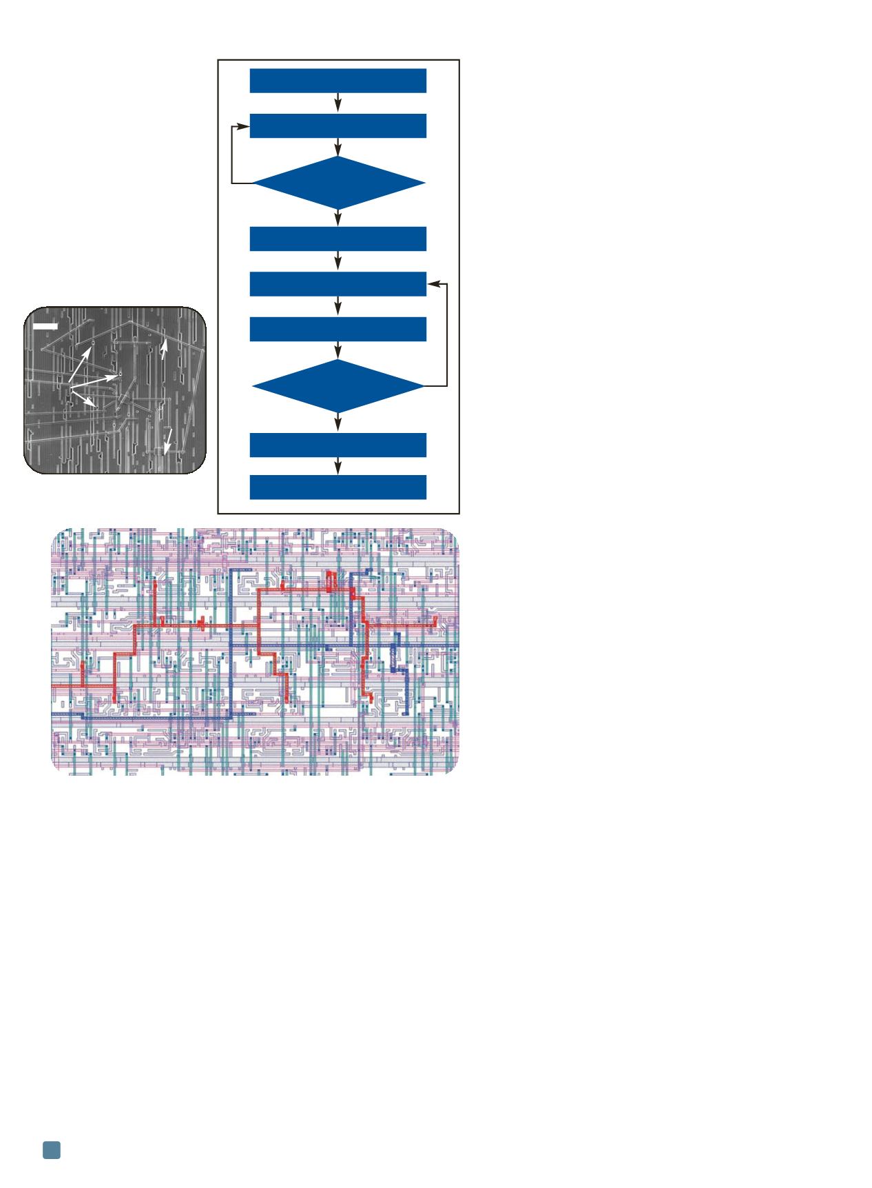
Another critical aspect is having a comprehensive
methodology and workflow (Fig. 2), beginning with a def-
inition of the electrical failure signature and continuing
through failure mechanism identification and problem res-
olution. In order to address multiple complex and interde-
pendent components and features, the process must also
be periodically disciplined and refined based on data and
incremental findings. This typically involves developing
hypotheses and then working to validate or reject them.
Various experiments may also be necessary in order to du-
plicate or model a given failure.
Customizing the failure analysis approach is also criti-
cal. Each situation has its own specific characteristics and
issues to address, and requires a methodical approach that
begins with the right questions in order to develop a cus-
tomized workflow.
Preventing IC failures before they occur
Another strategy to decrease failures is to thoroughly
test ICs and follow-up use of FIB circuit edit during the de-
velopment process, especially at advanced process nodes
where it would be difficult, if not impossible, to anticipate
future problems based on previous design work. Electrical
characterization, functional testing, and reliability qualifi-
cation can help uncover many issues before the produc-
tion stage. Once issues are identified, FIB circuit edit can
be used during the process of debugging and validating
fixes to in-progress designs, or design optimization
changes can be explored before committing to the high
cost and lengthy timetables of a full mask spin.
Barriers to success can be even higher at advanced
process nodes because of high mask costs and greater dif-
ficulty associated with finding and fixing bugs. It can be
extremely difficult to anticipate problems at these nodes
based on experience gained during earlier design work.
Devices manufactured at today’s 20-nm process nodes
have 10 times smaller feature sizes than the laser light
wavelength that is generally used in lithography. At these
advanced nodes, pre-silicon testing is more difficult, sim-
ulations take much longer, and it is impossible to fully ver-
ify many designs. Even more problematic are extremely
complex designs that may have flawed simulation models,
and which can easily be stressed by packaging.
With each new technology node, design and integra-
tion complexity grows. Challenges range from multiple
patterning and layout-dependent effects (LDE) to the use
of local interconnect layers. Server signals and power elec-
tro-migration can also create difficulties. The smaller the
metal pitch becomes, the more chance of coupling effects
and signal integrity issues. Higher wire and via resistance
also requires more advanced and variable wire sizing and
tapering techniques. There are also challenges related to
extraction, timing, signal integrity analysis, and modeling,
and each must account for many variation issues in order
to ensure accuracy without jeopardizing performance.
Plus, lithography limitations at 20 nm often create the need
for significant fixing in order to achieve signoff. Finally,
there are many different chip and intellectual property (IP)
integration challenges, packaging issues, and additional
ADVANCED MATERIALS & PROCESSES •
AUGUST 2014
24
Define failure signature
Develop initial analysis approach
Verify failure
Perform nondestructive analysis
Refine analysis approach
Disassemble
Fault localization
Identify failure mechanism and
root cause
Conclusion
Fig. 2 —
System-level failure
analysis methodology
and workflow.
Fig. 3 —
Multiple front-side
FIB circuit edit connections
and cuts.
Fig. 4 —
CAD layouts enable operators to perform FIB circuit edit.
15 µm
W connection
Cut
Insulator SiO
2