


 29 / 82

A D V A N C E D
M A T E R I A L S
&
P R O C E S S E S |
M A Y / J U N E
2 0 1 7
2 9
spectrum, SDDs can typically produce
equivalent if not better data in less
than 10 seconds. This makes sample
inspection much more immediate and
interactive. An added benefit of using
a lower beam current is that in some
SEMs, it can greatly improve imaging
resolution as well.
SEM/EDS DEMONSTRATION
To demonstrate the combined ca-
pabilities of SEM, EDS, and SDD tech-
nology, the author prepared and tested
two glass samples, the results of which
are presented below. The first sample is
a coated glass cover slip meant to be at-
tached as a protective layer over an ex-
isting cell phone display. In preparation
for the test, pieces of the cover slip were
mounted on edge in epoxy and polished
to a smooth finish. Samples were then
coated with a thin layer of conductive
carbon to counter the unwanted charge
accumulation.
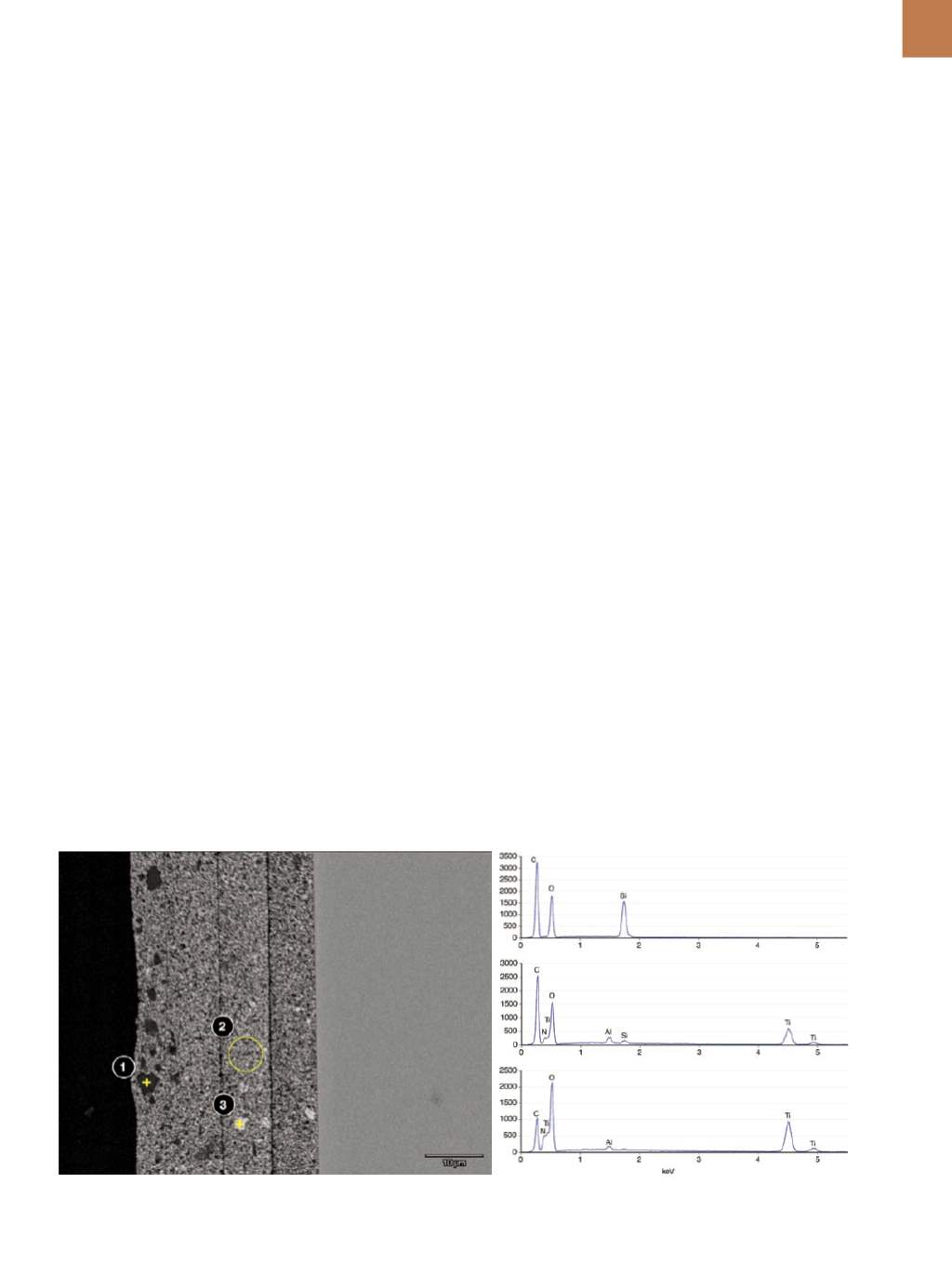
An electron image of the cover slip
is shown in Fig. 1 along with composi-
tional spectra from three selected ar-
eas. Typical of EDS spectra, the graphs
have a low-intensity background with
a few sharp peaks characteristic of spe-
cific elements. System software can
usually identify most peaks in a given
spectrum, and often provides the op-
tion of charting intensities as simple
counts, weights, or atomic percentages.
another version emerged that takes ad-
vantage of a sensing mechanism based
on fully depleted high-resistivity silicon.
These newer devices, called silicon-drift
detectors (SDDs), have very low leakage
current and can therefore operate close
to room temperature. Besides elimi-
nating the need for cryogenic cooling,
SDDs are also faster, more scalable, and
available in a wider range of sizes.
Using energy dispersive x-ray
spectroscopy to analyze cell phone cov-
er glass—even with the improvements
in detector technology—still requires
a fair amount of caution and care. For
one thing, cover glass contains sodium
ions that can become mobile when ex-
posed to a strong electron beam. Any
subsequent changes in composition
could lead to false measurements if not
accounted for. Cover glass is also non-
conductive and must be modified to
prevent unwanted buildup of charge
during scans. This is typically done by
coating the test sample with a thin layer
of conductive material such as carbon,
iridium, or another metal. Even then,
it is still possible for residual charge to
accumulate beneath the coating if the
electron beam intensity is not carefully
monitored.
GET THE DRIFT
Silicon drift detectors effectively
mitigate many of the challenges pre-
sented by cell phone cover glass be-
cause they work faster and at lower
beam currents than other detector
types. SDDs with digital pulse proces-
sors operate with much less overhead
than Si(Li) detectors, achieving signifi-
cantly higher x-ray count rates. Today’s
silicon drift detectors can easily reach
rates of 50,000 to 100,000 counts per
second if sufficient signal is provided
and if the sample can withstand the in-
tensity of beam current exposure. Sil-
icon-lithium versions, by comparison,
are limited to about 3000 counts per
second.
SDDs are also available in sizes of
up to 100 mm
2
or more, which is any-
where from three to 10 times larger
than Si(Li) detectors. And unlike their
predecessors, SDDs see little degrada-
tion in resolution as their active area
is increased. In fact, the largest SDDs
are rectangular in shape, which allows
them to get closer to the test sample
where they can capture more x-ray sig-
nal for a given beam intensity.
The bottom line for manufacturers
of cell phone cover glass is that, with
the right SDDs, they can now obtain
detailed compositional information
about their products without having
to crank up beam intensity to where
it could damage or alter the test sam-
ple—and they can do it in a fraction of
the time that it would have taken in the
past. Where Si(Li) detectors might need
almost two minutes to acquire a single
Fig. 1
– Electron image of glass cover slip cross section revealing surface layers and glass substrate. The three spectra were acquired from the
indicated locations in the surface coatings.
#1
#2
#3