


 30 / 82

A D V A N C E D M A T E R I A L S & P R O C E S S E S | M A Y / J U N E 2 0 1 7
3 0
a carbon-rich binder. The smallest dis-
cernable particles are roughly 100 nm
in diameter.
X-ray maps of the cell phone glass
are shown in Fig. 4. As before, left-to-
right line profiles for sodium and po-
tassium are superimposed on the SEM
image. It is clear that sodium and po-
tassium are distributed differently in
the two samples. In the glass slip, po-
tassium is concentrated at the surface
of the substrate, but in the phone glass,
it is observed in high levels to a depth of
more than 25 microns—indicative of a
wider region of ion-exchange strength-
ening. The sodium concentration, as
expected, rises as the potassium con-
centration falls. Note that there is little
or no change in the appearance of the
glass in the electron image, indicating
the presence of the potassium-rich re-
gion. Without EDS analysis, the depth,
intensity, and shape of the enhanced
potassium region would have gone
unnoticed.
The silicon map in the lower left
quadrant of the small image group re-
veals the presence of silicon (apparent-
ly SiO
2
particles) in the first of the four
coating layers. Titanium is distribut-
ed evenly throughout the layers as are
carbon, oxygen, and nitrogen. No oth-
er major constituent or particle was
found.
In the SEM image, the cover slip
surface is oriented to the left. The black
area is the epoxy and to the right of that
are four surface layers followed by the
glass substrate. The bright particles
scattered throughout the top layers
are found to be rich in titanium and the
darker particles rich in silicon. In this
type of image, the brighter the area, the
larger the average atomic number of
the sample.
Based on the analysis, the surface
coatings consist primarily of titanium,
carbon, oxygen, and nitrogen. The large
dark particles embedded in the top lay-
er are most likely composed of silicon
dioxide. If there were any contaminants
or inclusions in the sample, they would
be visible in the image.
DELVING DEEPER
A similar image of the cover slip
along with a corresponding x-ray map is
shown in Fig. 2. The map was acquired
by scanning the electron beam across
the sample and capturing x-ray spectra
at each node of an imaginary grid. The
procedure is automated and can find
the distributions of all measurable ele-
ments without knowing their identities
in advance. During the procedure, a live
view of the map is displayed. Afterward,
the spectra can be processed to reveal
additional sample details.
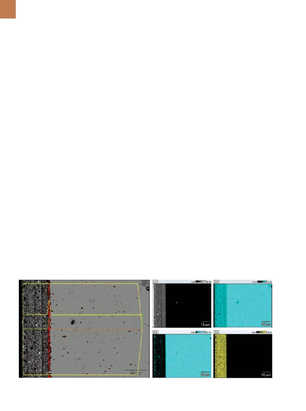
The red overlay on the SEM image
in Fig. 2, a potassium distribution map,
is an example of such post-processing.
It reveals a thin layer of potassium,
about one micron thick, at the surface
of the glass. The layer is rather nonuni-
form, alternating between areas of high
concentration and areas with no po-
tassium at all. Silicon-rich areas (likely
SiO
2
) are visible in the topmost layer,
while titanium, oxygen, and carbon are
distributed throughout.
Sodium and potassium distribu-
tion profiles were also extracted from
the test data and are included as over-
lays on the sample image. The yellow
trace represents potassium, while the
green trace is sodium. Note how sodi-
um concentration drops where potas-
sium peaks. The potassium line scan
was extracted from the full width of the
map; each point represents a vertical
column, which has an averaging effect
on variances in concentration.
SCREEN TEST
The other sample selected for the
demonstration is a piece of screen glass
from an actual cell phone. Like the cov-
er slip, it was mounted, polished, and
coated prior to scanning. An SEM im-
age and three compositional spectra
are shown in Fig. 3. As before, the sur-
face is oriented to the left and there are
four layers topping the substrate. The
surface layers again contain particles of
what appears to be SiO
2
and combina-
tions of titanium, nitrogen, oxygen, and
Fig. 2
– Electron image and EDS maps from the glass cover slip cross section. Overlaid on the electron image are extracted line scans for potassium
and sodium and the potassiummap.