


 31 / 82

A D V A N C E D
M A T E R I A L S
&
P R O C E S S E S |
M A Y / J U N E
2 0 1 7
3 1
CONCLUSION
SEM and EDS are effective tools for
visualizing the appearance and compo-
sition of materials in extremely precise
detail. With recent improvements in
silicon drift detectors—even with chal-
lenging samples that are fragile, non-
conducting, or prone to decomposing
when exposed to an electron beam—
analysis can be done safely, quickly, and
in some cases, interactively.
~AM&P
For more information:
John Konopka
is a microanalysis applications scientist
for Thermo Fisher Scientific, 525 Verona
Rd., Madison, WI 53711, 650.576.2312,
john.konopka@thermofisher.com,
www.thermofisher.com/pathfinder.
Reference
1. M.S. Tite and M. Bimson, Glazed
Steatite: An Investigation of the
Methods of Glazing Used in Ancient
Egypt,
World Archaeology
, Vol 21, No. 1,
p 87-100, 1989.
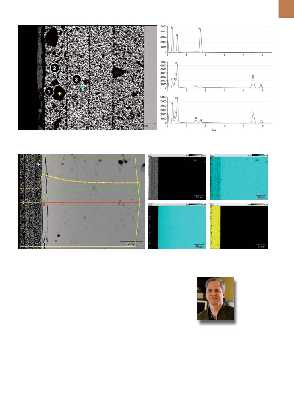
Fig. 3
– Image of a cross section of the cell phone glass surface, showing four surface coatings. The three spectra were acquired from the indicated
locations.
Fig. 4
– Electron image and EDS x-ray maps from a cross section of the cell phone glass surface. Extracted line scans for sodium and potassium are
overlaid on the electron image.
Konopka
#1
#2
#3