


 15 / 82

A D V A N C E D
M A T E R I A L S
&
P R O C E S S E S |
N O V E M B E R / D E C E M B E R
2 0 1 6
1 5
SURFACE ENGINEERING
ROOM-TEMPERATURE ATOMIC
LAYER DEPOSITION
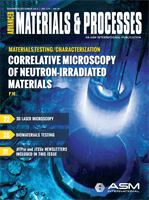
Researchers at the University of
Colorado Boulder developed a new
approach for synthesizing ultrathin ma-
terials at room temperature—a break-
through over industrial approaches that
require temperatures of 800°C or more.
The advance opens a path to creating a
host of previously unattainable thin-film
microelectronics, whose production by
conventional methods has been impos-
sible because many components lose
their critical functions when subjected
to high temperatures.
The new method is known as elec-
tron-enhanced atomic layer deposition
and was recently developed as part
of DARPA’s Local Control of Materials
Synthesis program. The team demon-
strated room-temperature deposition
of silicon and gallium nitride as well as
the ability to controllably etch specific
materials, leading to precise spatial
control in 3D.
colorado.edu.
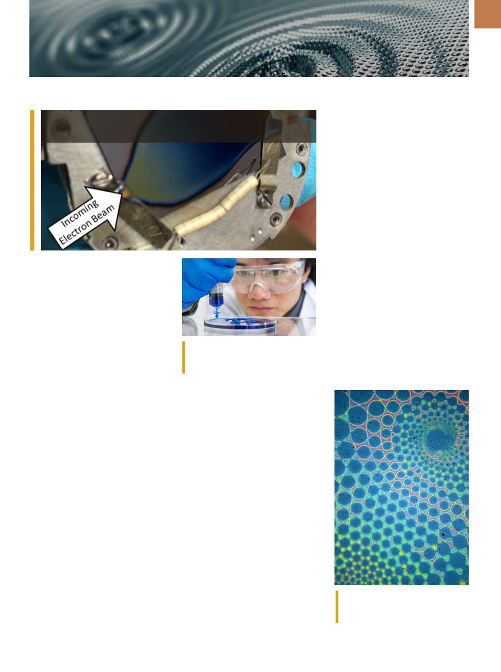
SPRAY-ON WATER PROOFING
Scientists at The Australian
National University (ANU) developed a
new spray-on material with a remark-
able ability to repel water. The coating
could eventually be used to waterproof
mobile phones, prevent ice from
forming on airplanes, and protect boat
hulls from corroding. The team com-
bined two plastics, one tough and one
flexible. “It’s like two interwoven fishing
nets, made of different materials,” says
Ph.D. student WilliamWong. The super-
hydrophobic coating is also transparent
and extremely resistant to ultraviolet
radiation.
www.anu.edu.au.
CREATING POLYMER BRUSHES
FOR ENGINEERED SURFACES
At the University of California,
Santa Barbara, researchers are looking
to greatly improve on polymer brush cre-
ation with a method of micron-scale sur-
face chemical patterning that not only
decreases the time and money spent
in manufacturing, but also adds versa-
tility to designs. Their method, called
“sequential stop-flow photopatterning,”
Galliumnitride film is deposited on silicon substrate at 27°C (80°F) using an
innovative process for depositing super thin films. Courtesy of University of
Colorado Boulder.
Scientists at ANU developed a new spray-
on, water-repellant material. Courtesy of
Stuart Hay/ANU.
features a new platform for functional-
izing and engineering surfaces with pat-
terned polymer brushes.
To create the brushes, a substrate
(with initiating molecules deposited)
is enclosed in a stop-flow cell and a
solution streamed in. Irradiation with
light can then initiate the reaction. A
separate photomask is positioned over
the top of the cell, allowing only some
light-activated growth. Next, the light is
turned off, the first solution is drained
from the cell, and a second one is
flowed in to functionalize the polymers.
Because neither the mask nor the sub-
strate has been moved, only the mole-
cules that have been exposed to light
are grown and functionalized. These
basic steps may be repeated with varia-
tions in the reactants, light source, sub-
strate positions, or photomask to create
polymer brush patterns in a single con-
tinuous process.
For more information:
Christian Pester,
pester@mrl.ucsb.edu,
www.ucsb.edu.
The stop-flow photopatterning method
enables intricate polymer brush patterns.
Courtesy of Christian Pester.