


 12 / 78

POLYMER, EAT MY DUST
Researchers at the Yale School
of Engineering and Applied Science,
New Haven, Conn., developed a non-
damaging method for removing dust
particles from surfaces using a poly-
mer film. When elastic, nonstick poly-
dimethylsiloxane (PDMS) is tapped
against an object, dust is attracted to
the polymer by electrostatic charge
and absorbed around millions of tiny
columns on the polymer’s surface. Col-
umns range in diameter from 2-50 µm—
although bigger particles require bigger
pillars. Laboratory tests on various sur-
faces show total cleaning of silica dust
particles and no damage to the object
being cleaned, even with dust parti-
cles smaller than 10 µm. Traditional
methods used to clean dust particles
this small are either only moderately
effective or can harm the objects being
cleaned.
In developing the new approach,
Yale postdoctoral associate Hadi Izadi
drew on his previous research into
the sticky mechanisms on gecko feet,
which also incorporate microscopic
pillars and electrostatic charge. Unlike
those micropillars, however, the ones
used for cleaning dust are specifically
designed not to be sticky. While PDMS
produces enough electrostatic charge
to detach dust from a surface, it has
minimal interaction with the surface
itself. The polymer method could be a
potential boon to aerospace engineers,
the electronics industry, and art conser-
vators, among others.
yale.edu.
NEW TOPOLOGICAL METAL
COULD QUICKEN COMPUTING
Physicists at the DOE’s Ames Lab-
oratory, Iowa, discovered a topologi-
cal metal composed of platinum and
tin (PtSn
4
) with a unique electronic
structure that could lead to advances
in computing speed. Electrons in topo-
logical quantum materials can travel
close to the speed of light due to a
unique property called
Dirac dispersion.
Until now, only isolated points—Dirac
points—with relatively small numbers
of conduction electrons were known to
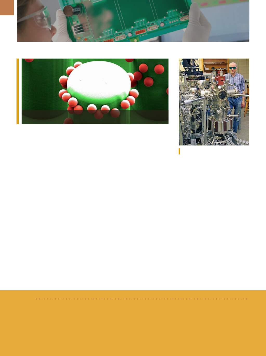
Microscopic images of silica dust particles lifted by micropillars, 50 µm in diameter.
Courtesy of Vanderlick Lab.
AdamKaminski and his ARPES equipment.
BRIEF
An independent nonprofit founded by
Massachusetts Institute of Technology,
Cambridge, was selected to lead a
new, $317 million public-private partnership called the Advanced Functional Fabrics of America Institute (AFFOA),
designed to accelerate innovation in high-tech, U.S.-based manufacturing involving fibers and textiles. AFFOA
includes 32 universities, 16 industry members, 72 manufacturing entities, and 26 startup incubators spread across
27 states and Puerto Rico.
mit.edu.
exist in such materials. In PtSn
4
, how-
ever, scientists not only discovered a
high density of conduction electrons,
but also a large number of closely posi-
tioned Dirac points forming extended
lines, or Dirac node arcs.
“This type of electron transport is
very special,” explains Adam Kaminski,
professor of physics and astronomy at
Iowa State University. “Our research
has been able to associate the extreme
magnetoresistance with novel features
in their electronic structure, which
may lead to future improvements in
computer speed, efficiency, and data
storage.” The discovery was made
using a device that Kaminski devel-
oped at Ames—a laser-based, angle-
resolved photoemission spectroscopy
(ARPES) instrument that provides high-
resolution details of the electronic
properties of materials.
ameslab.gov.EMERGING TECHNOLOGY
A D V A N C E D M A T E R I A L S & P R O C E S S E S | J U N E 2 0 1 6
1 2