


 17 / 78

A D V A N C E D
M A T E R I A L S
&
P R O C E S S E S | J A N U A R Y
2 0 1 6
1 7
NANOTECHNOLOGY
BRIEFS
Aleris, Cleveland, offers a new 7017 aluminum alloy in North America for commercial plate and defense
uses. After extensive review and testing, the U.S. Army Research Lab issued MIL-DTL-32505 for use in armor
applications. 7017 offers high strength, good weldability, and corrosion resistance. It is currently used in
Europe and Asia on combat vehicles to achieve superior ballistic protection.
aleris.com.
GRAPHENE BOOSTS
DESALINATION EFFICIENCY
The laboratory of Jeffrey Gross-
man, a professor at Massachusetts In-
stitute of Technology, Cambridge, has
demonstrated strong results showing
that new filters made from graphene
could greatly improve the energy effi-
ciency of desalination plants while po-
tentially reducing other costs as well.
At only an atom thick, there is far less
friction loss when you push seawater
through a perforated graphene filter
compared with the polyamide plastic
filters that have been used for the last
50 years, says Grossman.
“The process of pumping seawater
through filters represents about half the
operating costs of a desalination plant.
With graphene, we could use 15% less
energy for seawater and up to 50% less
energy for brackish water,” he explains.
Another advantage is that graphene
filters do not become fouled with bio-
growth at nearly the rate that occurs
with polyamide filters. In addition, the
chlorine used to clean the filters reduc-
es the polyamide’s structural integrity,
requiring frequent replacement. By
comparison, graphene is resistant to
the damaging effects of chlorine.
For
more information: Jeffrey Grossman,
617.324.3566,
jcg@mit.edu , mit.edu.
BORON-DOPED GRAPHENE
ENABLES SUPER SENSITIVE
SENSORS
Graphene is known for its remark-
able strength and ability to transport
electrons at high speed, but it is also a
highly sensitive gas sensor. In a study
conducted by an international research
team, graphene sensors with the addi-
tion of boron atoms detected noxious
gas molecules at extremely low concen-
trations, parts per billion in the case of
nitrogen oxides and parts per million for
ammonia. This translates to 27
×
great-
er sensitivity to nitrogen oxides and
10,000
×
greater sensitivity to ammonia
compared to pristine graphene. Re-
searchers from Pennsylvania State Uni-
versity, State College, and colleagues
believe these results will enable devel-
opment of high-performance sensors
that can detect trace amounts of many
other molecules. These sensors can be
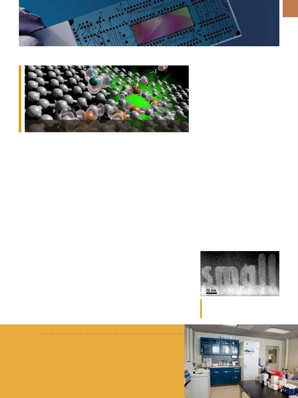
Drawing of boron-doped graphene. Courtesy of Terrones, Penn State.
Researchers use a new SEM technique to
sculpt 3D nanoscale features in a com-
plex oxide material. Courtesy of ORNL.
BRIEF
A 4000-sq-ft nanomaterials r s arch laboratory is opening at
Cornell
University,
Ithaca, N.Y. The
C nter for Nanom terials Engineering and
Technology (CNET)
includes equipment for mate ials synthesis, phys-
ical characterization, and sc le-up. The tools can be used to develop
and analyze materials for applications including carbon capture and
conversion, electrochemical energy storage in batteries, and hydrogels
for biomedicine and drug delivery.
cnet.research.engineering.cornell.edu.
used for labs and industries that use
ammonia or need to detect nitrogen
oxides.
psu.edu.
USING ELECTRON
MICROSCOPES TO
BUILD 3D STRUCTURES
Researchers at the Department of
Energy’s Oak Ridge National Laborato-
ry, Tenn., have developed a unique way
to build 3D structures with finely con-
trolled shapes as small as one to two
billionths of a meter. The study demon-
strates how scanning transmission
electron microscopes, normally used as
imaging tools, are also capable of pre-
cision sculpting of nanometer-sized 3D
features in complex oxide materials. By
offering single atomic plane precision,
the technique could find use in fabricat-
ing structures for functional nanoscale
devices such as microchips. The struc-
tures grow in perfect crystalline align-
ment, which ensures that the same
electrical and mechanical properties
extend throughout the whole material.
ornl.gov.