


 18 / 102

A D V A N C E D M A T E R I A L S & P R O C E S S E S | O C T O B E R 2 0 1 5
1 8
NANOTECHNOLOGY
FABRICATING SILVER
NANOPARTICLES AT ROOM
TEMPERATURE
Engineers at Oregon State Univer-
sity, Corvallis, invented a way to fab-
ricate silver for printed electronics at
room temperature. “There’s a great deal
of interest in printed electronics, be-
cause they’re fast, cheap, can be done
in small volumes and changed easily,”
says engineering professor Chih-hung
Chang. “But the heat needed for most
applications of silver nanoparticles has
limited their use.”
Scientists solved that problem by
using a microreactor to create silver
nanoparticles at room temperatures
without any protective coating, and
then immediately printing them onto
almost any substrate with a contin-
uous flow process. “Because we can
now use different substrates such as
plastics, glass, or even paper, these
electronics could be flexible, very inex-
pensive, and stable,” Chang says. “This
could be quite important and allow
silver use in many types of electronic
applications.”
For more information:
Chih-hung Chang, 541.737.8548,
chih- hung.chang@oregonstate.edu,www. oregonstate.edu
.
POLYMER MOLD PROMISES
PERFECT NANOSTRUCTURES
For molds to work, they must be
stable while hot liquid materials hard-
en into shapes. In a breakthrough for
nanoscience, polymer engineers at Cor-
nell University, Ithaca, N.Y., made such a
mold for nanostructures that can shape
liquid silicon out of an organic polymer
material, paving the way for perfect, 3D,
single crystal nanostructures.
The advance comes from the lab
of Professor Uli Wiesner, whose prior
work involved creating novel materials
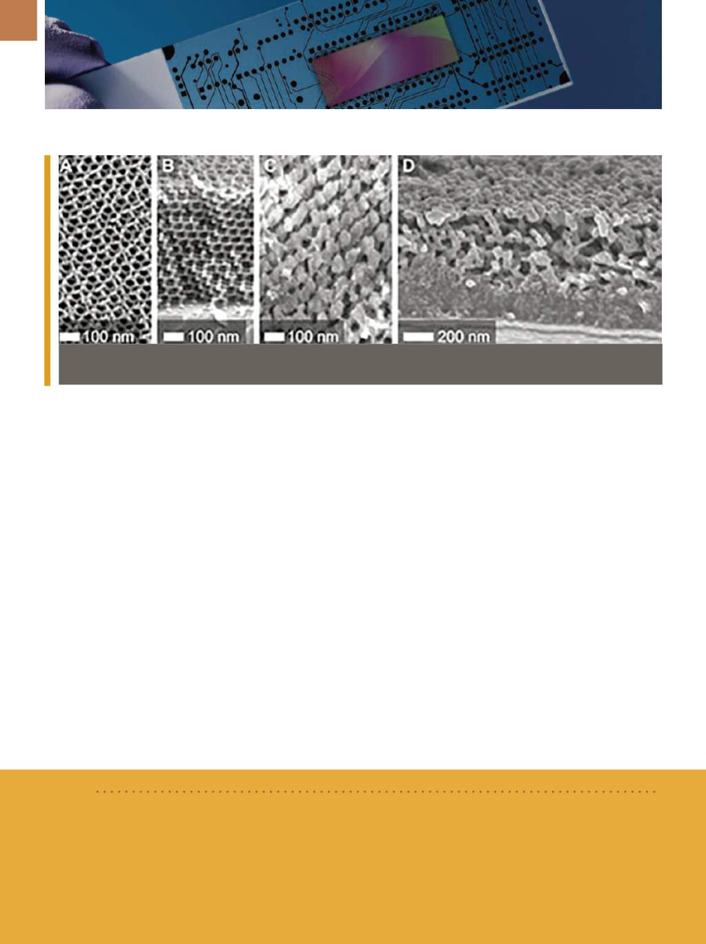
Scanning electron microscopy micrographs of a periodically orderedmesoporous gyroidal resin template (A, B) and the resulting
laser-induced crystalline silicon nanostructure after template removal (C, D).
BRIEF
ASTM International,
West Conshohocken, Pa., recently published two standards that educate workers about the
nanotechnology industry: E2996
, Guide for Workforce Education in Nanotechnology Health and Safety,
and E3001,
Practice for Workforce Education in Nanotechnology Characterization.
E2996 provides an overview of health and safety
aspects of nanotechnology, describing the minimum knowledge base needed for an individual involved in nanoman-
ufacturing or nanomaterials research.
astm.org.
made of organic polymers. With the
right chemistry, organic polymers
self-assemble, and researchers used
this special ability of polymers to make
a mold dotted with precisely shaped
and sized nanopores. Normally, melting
amorphous silicon, which has a melting
temperature of about 2350°F, would de-
stroy the delicate polymer mold, which
degrades at about 600°F. The scientists
overcame this by using extremely short
melt periods induced by a laser. The
polymer mold holds up if the silicon is
heated by laser pulses just nanosec-
onds long. At such short time scales,
silicon can be heated to a liquid, but
the melt duration is so short the poly-
mer doesn’t have time to oxidize and
decompose. Researchers essentially
tricked the polymer mold into retain-
ing its shape at temperatures above its
decomposition point.
For more informa-
tion: Uli Wiesner, 607.255.3487,
ubw1@ cornell.edu,
www.cornell.edu.