


 20 / 70

news
industry
Discovery of 2D structures with unique properties
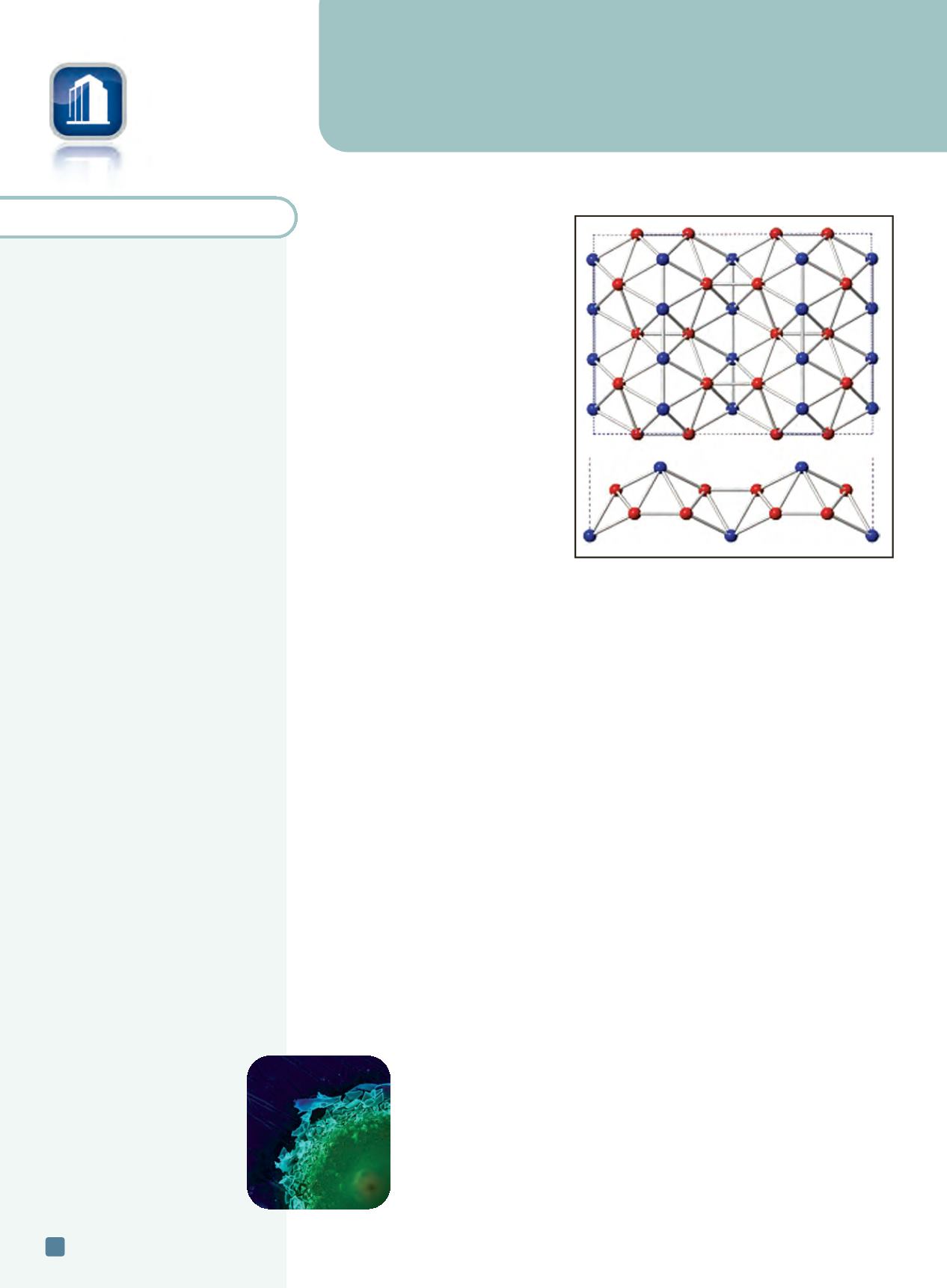
Researchers at Stony Brook Uni-
versity, N.Y., discovered the structure
of 2D boron crystals, which is rele-
vant to electronic applications and to
understanding boron nanostruc-
tures. “Boron is in many ways an ana-
log of carbon,” says Xiang-Feng Zhou.
“Its nanostructures—nanoparticles,
nanotubes, and two-dimensional
structures—have attracted a lot of in-
terest in the hopes of replicating, or
even surpassing, the unique proper-
ties and diversity of carbon nano-
structures. Our findings overturn the
assumptions and predictions of nu-
merous previous studies.” Flat mono-
layer structures of boron were found
to be extremely unstable, and the ac-
tual structures have finite thickness.
These findings will likely lead to a re-
vision of structural models of boron
nanoparticles and nanotubes. In particular, it is possible that hollow, fullerene-like struc-
tures will be unstable for boron.
www.stonybrook.edu.
Electrochemical nanoceramic production line debuts
Cambridge Nanotherm, UK, installed the first of many fully automated lines to produce
Nanotherm ceramic, which is grown on the surface of aluminum to create a dielectric layer
directly on the surface of an aluminum substrate. The nanoceramic dielectric layer is re-
portedly between two and 10 times thinner than the competition and achieves thermal re-
sistance of 0.014
o
Ccm
2
/W. The dielectric has a thermal conductivity of 7 W/mK, which is
two to three times more effective at heat dissipation than conventional MB PCB (metal
back printed circuit board) dielectric materials. The first application of this technology is
effective heat dissipation for LED lighting, which reduces operating temperatures by 20%
to extend LED life or make it more energy efficient.
www.camnano.com.
Sea creatures inspire ceramic-based armor
Researchers at Massachusetts Institute of Technology, Cambridge, analyzed the shells
of a sea creature, mollusk Placuna placenta, to determine exactly why they are so resistant
to penetration and damage—even though they are 99% calcite, a weak, brittle mineral. The
shells’ unique properties emerge from a specialized nanostructure that allows optical clar-
ity, as well as efficient energy dissipation and the ability to localize deformation.
Engineered ceramic-based armor, while designed to resist penetration, often lacks the
ability to withstand multiple blows, due to large-scale deformation and fracture that can
compromise its structural integrity, says professor Christine Ortiz. The properties of this
natural armor make it a promising template for the development of bio-in-
spired synthetic materials for both commercial and military applications—
such as eye and face protection for soldiers, windows and windshields, and
blast shields, Ortiz explains.
For more information: Christine Ortiz, 617/452-
3084,
cortiz@mit.edu,
www.dmse.mit.edu.
Transmission electron microscope image shows the region surrounding an
indentation researchers made in a piece of shell from Placuna placenta. The
image shows the localization of damage to the area immediately surrounding the
stress. Courtesy of Ling Li/MIT.
ADVANCED MATERIALS & PROCESSES •
MAY 2014
20
N
ANOTECHNOLOGY
briefs
The
National Science and
Technology Council,
Washington,
released the
2014 National
Nanotechnology Initiative (NNI)
Strategic Plan,
which aims to
ensure that nanotechnology
advances and applications
continue. It also addresses
potential concerns about future
and existing applications. The plan
is a guide for agency leaders,
program managers, and the
research community regarding
design and implementation of
nanotechnology R&D investments
and activities.
http://nano.gov/node/1089.Applied Nanotech Holdings Inc.,
Austin, and
NanoHolding Inc.,
the
parent company of
Nanofilm Ltd.,
will merge to create a new
company named
PEN Inc.
The new entity will build a platform
for a higher rate of expected
revenue growth, based on
increased capabilities in
intellectual property, personnel,
development facilities, operating
facilities, and customer relations to
pursue product commercialization.
www.appliednanotech.net.
The
V-SMMART Nano
(volumetric
scanning microwave microscope
analytical and research tool for
nanotechnology) project aims to
develop a new tool for subsurface
analysis that will push the
measurement of subsurface
structures at the nanoscale to new
limits. The consortium is
developing and will commercialize
a 3D hybrid scanning probe
microscope platform able to probe
the local reflection and
transmission of microwaves from
samples. It will then reconstruct
the subsurface 3D structure of the
materials from these signals, with
nanoscale resolution in the three
spatial dimensions.
www.vsmmartnano.com.
Projections of 2 × 2 × 1 supercell of Pmmn-boron
structure along [001] and [100] directions.