


 45 / 66

edfas.org
45
ELECTRONIC DEVICE FAILURE ANALYSIS | VOLUME 18 NO. 4
GUEST EDITORIAL
CONTINUED FROM
PAGE 2
from the 130 nm to the 14 nm nodes. Solutions over this
period can be subdivided into those resulting from:
• Enhancement of existing analytical techniques
• Development/applicationof newanalytical techniques
• Development of new analysis approaches and/or
sample-preparation methodologies
An example of the enhancement of existing analytical
techniques lies in the introduction of spherical aberration
correction in scanning electronmicroscopy and transmis-
sion electron microscopy (TEM)/scanning transmission
electron microscopy (STEM). The fact that TEM/STEM are
projection techniques has pushed the need for tomog-
raphy and holography, with multiple approaches now
available. Note: Although thediffraction limit of TEM/STEM
is significantly smaller than that of atomic dimensions,
the spatial resolution noted in tomography/holography
now lies in the nanometer range.
Examples of the application of new techniques over
this period may have included, but are not limited to,
conductive atomic forcemicroscopy, scanning spreading
resistancemicroscopy, infrared atomic forcemicroscopy,
tip-enhanced Raman spectroscopy, and so on.
An example of a new analytical approach lies in the
application of large-area techniques over areas populated
with periodic repeating structures (for example, a sea of
fins over 50 by 50 µm areas or larger). These have been
found to be useful in providing data beyond the diffrac-
tion limit of the respective technique. Examples include
secondary ion mass spectrometry (SIMS) in the form of
1.5-D SIMS, x-ray diffraction, critical-dimension small-
angle x-ray scattering, and so on.
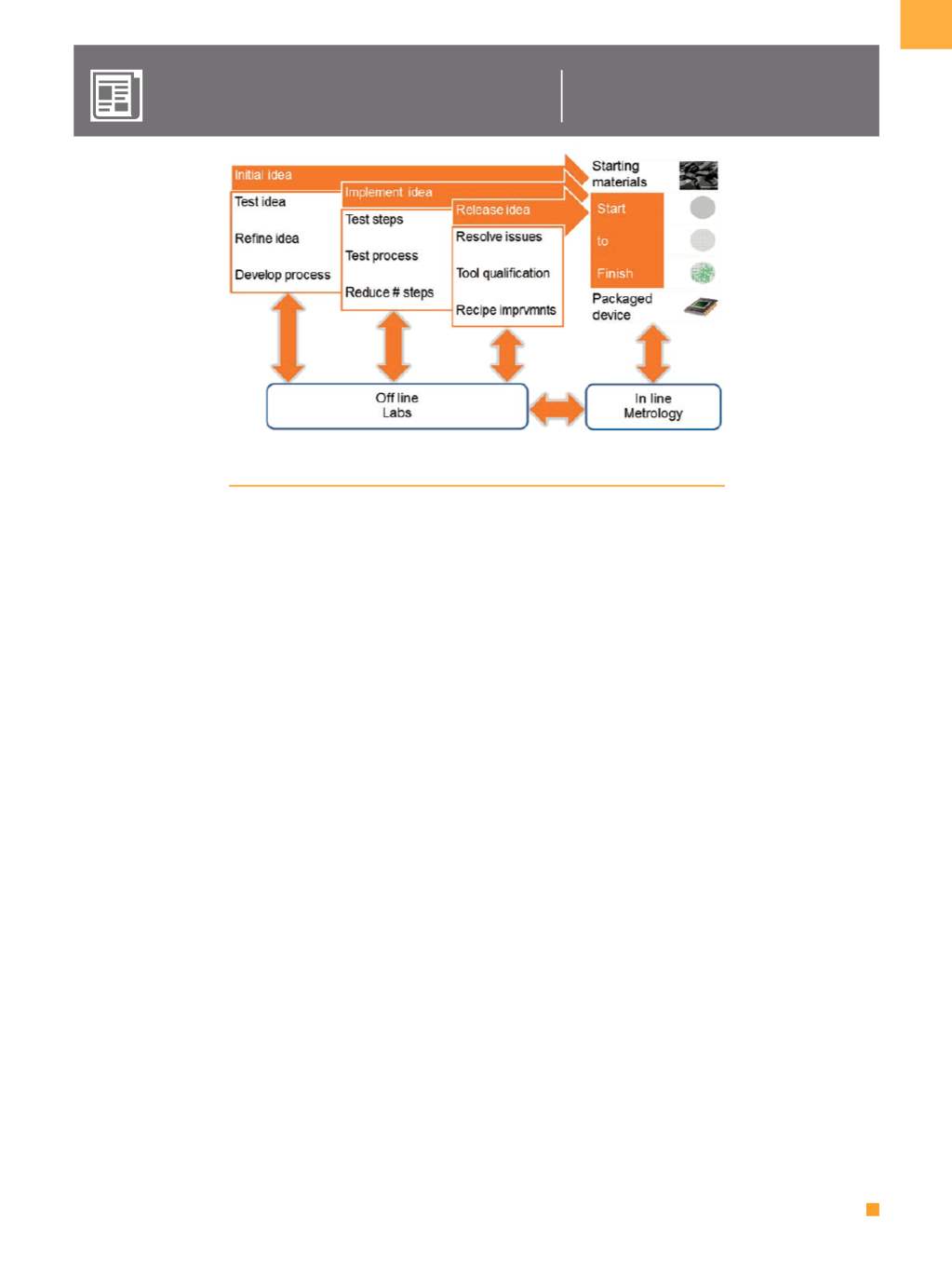
Fig. 1 Requirements of the FA labs in
supporting R&D efforts
The demands on the FA labs are then taken to the next
level if the respective HVM site is also involved in research
and development (R&D). This is realized because the
labs are critical in idea development through to process
implementation and refinement, as illustrated in Fig. 1.
The difference between the FA labs and metrology in this
figure stems from the fact that the former is involved in
process development (inclusive of evaluating newmateri-
als), process qualification, process refinement, through to
the examination of process issues, while the latter is pri-
marily concernedwith process control, with some degree
of issue/yield understanding also included (sometimes in
separate departments). This also brings into question the
terminology used (that of “FA labs”), as this would tend
to describe a subset of their overall scope, that is, implies
yield learning only as opposed to materials, device, and
process learning.
Alongwith the FA lab capabilities are the expectations
that the analytical techniques provide:
• High level of precision and repeatability
• Fast turnaround/cycle time
• Cost-effectiveness
• High uptime
Reasons for precision/repeatability lie in the fact that
the respective process step or steps must be controllable
to predefined upper and lower limits, which, in some
cases, reach subatomic dimensions. (Although interre-
lated, device response is dictated by electric fields, not
atomic dimensions.) The remaining three items can be
tied directly to the financial stakes in semiconductor HVM.