


 12 / 82

A D V A N C E D M A T E R I A L S & P R O C E S S E S | M A Y / J U N E 2 0 1 7
1 2
GRAPHENE OXIDE
CHANGES CHARGE
Scientists at North Carolina State
University, Raleigh, developed a meth-
od for changing positively charged
(p-type) reduced graphene oxide (rGO)
into negatively charged (n-type) rGO,
producing a layered material that could
be used in transistors for next-gener-
ation electronic devices. “Graphene
is extremely conductive, but is not a
semiconductor. Graphene oxide has
a bandgap like a semiconductor, but
does not conduct well,” explains Jay
Narayan, professor of materials science
and engineering. To harness both of
these desired qualities, the researchers
created rGO. However, rGO is p-type.
They needed to find a way to create
n-type rGO as well, in order to use the
material for p-n junction-based 2D elec-
tronic devices.
To make n-type rGO,
Narayan and his team first
integrated p-type rGO across
a sapphire and silicon wafer.
Then they used high-pow-
ered
nanosecond
laser
pulses to disrupt chemical
groups at regular intervals
across the wafer, moving
electrons from one group
to another—effectively con-
verting some of the p-type
rGO to n-type rGO. The laser
radiation annealing provided
a high degree of spatial and
depth control for creating
the necessary n-type regions
and the entire process took
place at room temperature in less than
one-fifth of a microsecond. The end re-
sult was a wafer with a layer of n-type
rGO on the surface and a layer of p-type
rGO underneath. This is critical because
the p-n junction—where the two types
meet—is what makes the material use-
ful for transistor applications in elec-
tronic devices.
ncsu.edu.
CUSTOMIZING ELECTRONIC
PROPERTIES, ATOM BY ATOM
By arranging individual atoms in
a lattice, scientists at Aalto Universi-
ty, Finland, created artificial materials
that deliver predetermined electrical
responses. Working at a temperature of
4 K, the researchers used a scanning
tunneling microscope to specifical-
ly place vacancies in a single layer of
chlorine atoms supported on a copper
crystal. They created two structures
Tip of a scanning tunneling microscope
above chlorine atoms. By moving
individual atoms under the microscope,
scientists were able to arrange vacancies
in a single layer of chlorine atoms and
create atomic lattices with a predeter-
mined electrical response. Courtesy of
Aalto University.
BRIEF
inspired by fundamental model sys-
tems with exotic electronic properties.
“The correspondence between
atomic structure and electronic prop-
erties is of course what happens in real
materials as well,” notes Robert Drost,
“but here we have complete control
over the structure. In principle, we
could target any electronic property
and implement it experimentally.” The
method is not limited to chlorine—the
same procedure could be applied in
many well-understood surface and
nanoscience systems. It could even be
adapted to mesoscopic systems, such
as quantum dots, which are controlled
through lithographic processes, paving
the way toward development of design-
er quantummaterials.
www.aalto.fi/en.
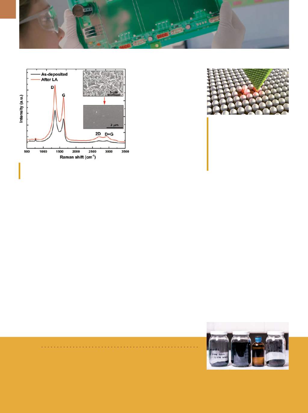
EMERGING TECHNOLOGY
Raman spectroscopy of the rGO thin films. LA is pulsed
laser annealing.
Gurpreet Singh, associate professor at
Kansas State University,
Manhattan,
created a clear liquid polymer with the viscosity and density of water that
changes into a black glasslike ceramic when heated. Composed of just five
ingredients—silicon, boron, carbon, nitrogen, and hydrogen—the material
possesses valuable thermal, optical, and electronic properties, and can be
mass-produced
. k-state.edu.Jars show variations of a patented liquid
polymer that looks like water but turns
into a ceramic when heated.
Courtesy of Kansas State.