


 15 / 86

A D V A N C E D
M A T E R I A L S
&
P R O C E S S E S |
A P R I L
2 0 1 6
1 5
NANOTECHNOLOGY
BRIEFS
Aleris, Cleveland, offers a new 7017 aluminum alloy in North America for commercial plate and defense
uses. After extensive review and testing, the U.S. Army Research Lab issued MIL-DTL-32505 for use in armor
applications. 7017 offers high strength, good weldability, and corrosion resistance. It is currently used in
Europe and Asia on combat vehicles to achieve superior ballistic protection.
aleris.com.
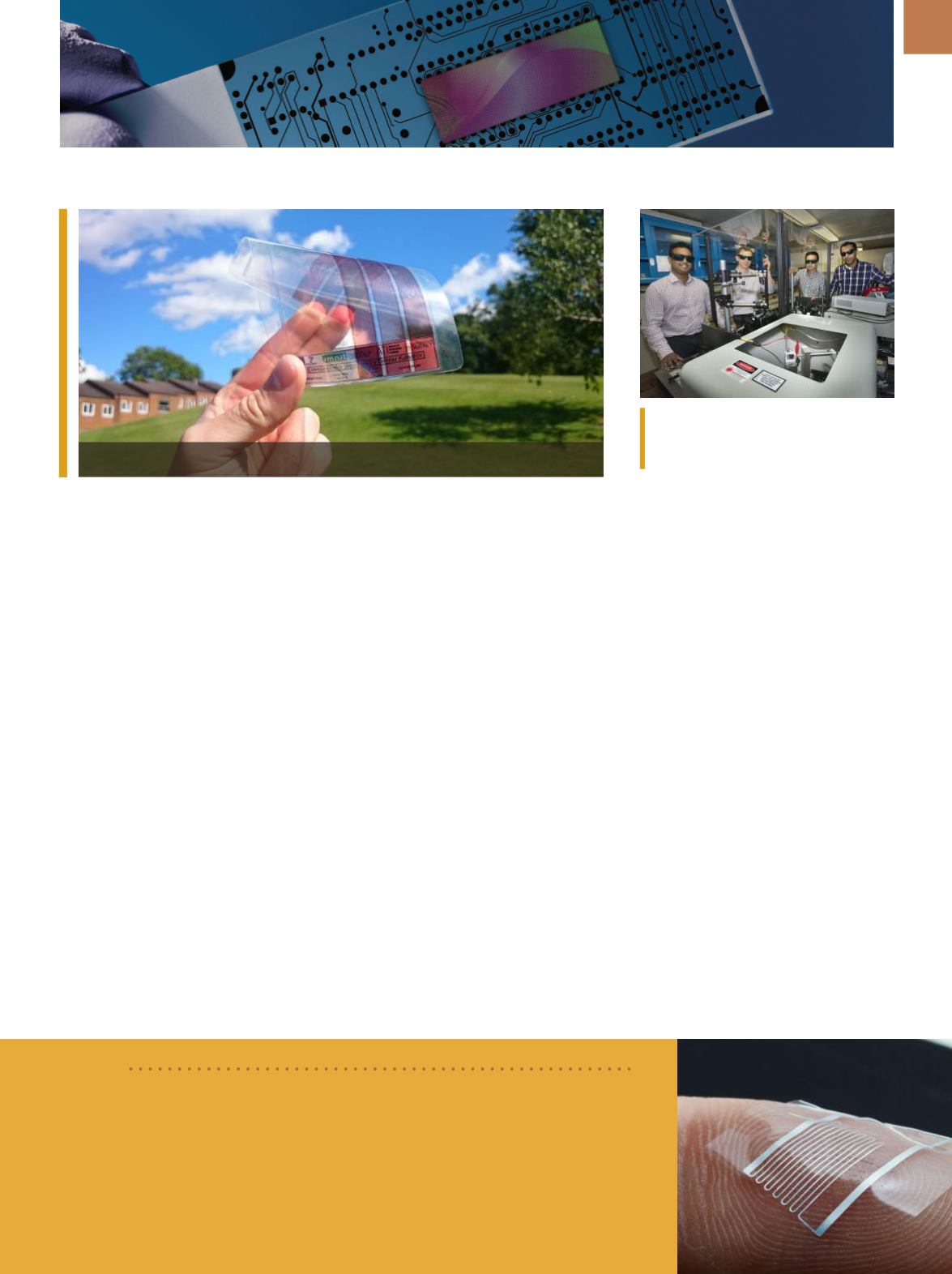
LIGHT ABSORBING GRAPHENE
PATTERNED AFTER NATURE
Using a technique known as nan-
otexturing, which involves growing
graphene around a textured metallic
surface, researchers from the Advanced
Technology Institute (ATI) at the Uni-
versity of Surrey, UK, created ultrathin
graphene sheets designed to more ef-
fectively capture light. Graphene has
remarkable electrical conductivity and
mechanical strength, but is tradition-
ally inefficient at light absorption. To
combat this, the team used nanopat-
terning to localize light into the narrow
spaces on the textured surface, increas-
ing the amount of light absorbed by
the material from 2-3% to about 95%
across a broad spectrum—from UV to
infrared.
The team takes its inspiration from
nature. “Moths’ eyes have microscopic
patterning that allows them to see in
the dimmest conditions. These work by
channeling light towards the middle of
the eye with the added benefit of elim-
inating reflections,” explains professor
Ravi Silva, head of the ATI. His group
used the same technique to pattern the
graphene. The material could be used
in a variety of applications from solar
cells that could harvest very dim light
to optoelectronic technologies.
www. surrey.ac.uk.
GRAPHENE GETS DOPED
UP ON GLASS
In an unexpected twist, research-
ers discovered a simple and powerful
way to create resilient, customized, and
high-performing graphene: Layer it on
top of common glass. This scalable and
inexpensive process helps pave the way
for a new class of microelectronic and
optoelectronic devices—from efficient
solar cells to touchscreens. The collab-
oration was led by scientists at the U.S.
Department of Energy’s Brookhaven
National Laboratory, Upton, N.Y.; Stony
From left, Nanditha Dissanayake, Mat-
thew Eisaman, Yutong Pang, and Ahsan
Ashraf in a laser lab at Brookhaven.
BRIEF
Researchers at the Écol
Polyt chnique Fédérale de Lausan e
(EPFL), Switzerland,
developed conductive tracks hat ca be b nt and str tched up to fou times their
original length. Unlike conventional conductive tracks that are usua ly hard printed on
a board, those developed at EPFL are alm st as fl xib as rubb r. They can undergo
amillion stretches without cracking or compromising conductivity, and could be used
in artificial skin, connected clothing, or on-body sensors.
www.epfl.ch.
Stretchable electronics from EPFL can quadruple in length.
Brook University, N.Y.; the U.S. Pho-
tovoltaic Manufacturing Consortium,
Albany, N.Y.; and SUNY Polytechnic
Institute, Albany, N.Y.
The team initially set out to opti-
mize a solar cell containing graphene
stacked on a semiconductor stacked
on a substrate of industrial soda-lime
glass, the type of glass commonly
found in windows and bottles. To max-
imize the graphene’s electronic prop-
erties, they planned to dope it, which
is typically done by introducing exter-
nal chemicals. However, preliminary
tests revealed that the graphene was
already optimally doped. After isolat-
ing the graphene on the glass, the team
discovered that the sodium in the sub-
strate automatically created high elec-
tron density within the multilayered
graphene. Crucially, the effect remained
strong even when the devices were ex-
posed to air for several weeks—a clear
improvement over competing doping
techniques.
science.energy.gov.Flexible solar cell. Courtesy of University of Surrey.